- 您現(xiàn)在的位置:買賣IC網(wǎng) > PDF目錄370849 > M37753FFCHP (Mitsubishi Electric Corporation) SINGLE CHIP 16 BIT CMOS MICROCOMPUTER FLASH MEMORY VERSION PDF資料下載
參數(shù)資料
| 型號: | M37753FFCHP |
| 廠商: | Mitsubishi Electric Corporation |
| 英文描述: | SINGLE CHIP 16 BIT CMOS MICROCOMPUTER FLASH MEMORY VERSION |
| 中文描述: | 單片微機16位CMOS閃存版 |
| 文件頁數(shù): | 19/67頁 |
| 文件大?。?/td> | 525K |
| 代理商: | M37753FFCHP |
第1頁第2頁第3頁第4頁第5頁第6頁第7頁第8頁第9頁第10頁第11頁第12頁第13頁第14頁第15頁第16頁第17頁第18頁當前第19頁第20頁第21頁第22頁第23頁第24頁第25頁第26頁第27頁第28頁第29頁第30頁第31頁第32頁第33頁第34頁第35頁第36頁第37頁第38頁第39頁第40頁第41頁第42頁第43頁第44頁第45頁第46頁第47頁第48頁第49頁第50頁第51頁第52頁第53頁第54頁第55頁第56頁第57頁第58頁第59頁第60頁第61頁第62頁第63頁第64頁第65頁第66頁第67頁
19
MITSUBISHI MICROCOMPUTERS
M37753FFCFP
M37753FFCHP
PRELIMINARY
Notice: This is not a final specification.
Some parametric limits are subject to change.
SHINGLE-CHIP 16-BIT CMOS MICROCOMPUTER FLASH MEMORY VERSION
Program command
The microcomputer enters the program mode by inputting command
code “40
16
” in the first cycle. The command code is latched into the
internal command latch at the rising edge of the WE input. When the
address which indicates a program location and data are input in the
second cycle, the M37753FFCFP and the M37753FFCHP internally
latch the address at the falling edge of the WE input and the data at
the rising edge of the WE input. The M37753FFCFP and the
M37753FFCHP start programming at the rising edge of the WE in-
put in the second cycle and finishes programming within 10
μ
s as
measured by its internal timer. Programming is performed in units of
bytes.
Note:
A programming operation is not completed by executing the
program command once. Always be sure to execute a pro-
gram verify command after executing the program command.
When the failure is found in this verification, the user must re-
peatedly execute the program command until the pass. Refer
to Figure 12 for the programming flowchart.
Program verify command
The microcomputer enters the program verify mode by inputting
command code “C0
16
” in the first cycle. This command is used to
verify the programmed data after executing the program command.
The command code is latched into the internal command latch at the
rising edge of the WE input. When control signals are input in the
second cycle at the timing shown in Figure 10, the M37753FFCFP
and the M37753FFCHP output the programmed address’s contents
to the external. Since the address is internally latched when the pro-
gram command is executed, there is no need to input it in the sec-
ond cycle.
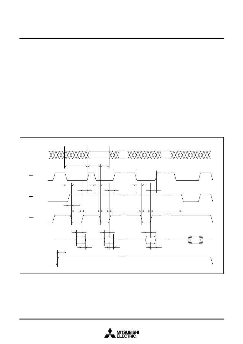
Fig. 10 Input/output timings during programming (Verify data is output at the same timing as for read.)
Address
Program
Program verify
Program
address
t
WC
t
CS
t
RRW
t
WP
t
WPH
t
WP
t
DP
t
DS
40
16
D
IN
C0
16
Dout
t
DS
t
DH
t
DH
Verify data output
t
DH
t
VSC
t
DS
t
WP
t
WRR
t
CS
t
CS
t
CH
t
CH
t
CH
t
AS
t
AH
V
IH
V
IL
V
IH
V
IL
V
IH
V
IL
V
IH
V
IL
V
IH
V
IL
V
PP
H
V
PP
L
CE
OE
WE
Data
V
PP
相關PDF資料 |
PDF描述 |
|---|---|
| M37754M8C-XXXGP | SINGLE-CHIP 16BIT CMOS MICROCOMPUTER |
| M37754M8C-XXXHP | SINGLE-CHIP 16BIT CMOS MICROCOMPUTER |
| M37754S4CGP | SINGLE-CHIP 16BIT CMOS MICROCOMPUTER |
| M37754S4CHP | SINGLE-CHIP 16BIT CMOS MICROCOMPUTER |
| M37754 | SINGLE-CHIP 16BIT CMOS MICROCOMPUTER |
相關代理商/技術參數(shù) |
參數(shù)描述 |
|---|---|
| M37753M6C-XXXFP | 制造商:RENESAS 制造商全稱:Renesas Technology Corp 功能描述:SINGLE-CHIP 16-BIT CMOS MICROCOMPUTER |
| M37753M6C-XXXHP | 制造商:RENESAS 制造商全稱:Renesas Technology Corp 功能描述:SINGLE-CHIP 16-BIT CMOS MICROCOMPUTER |
| M37753M8C-XXXFP | 制造商:RENESAS 制造商全稱:Renesas Technology Corp 功能描述:SINGLE-CHIP 16-BIT CMOS MICROCOMPUTER |
| M37753M8C-XXXHP | 制造商:RENESAS 制造商全稱:Renesas Technology Corp 功能描述:SINGLE-CHIP 16-BIT CMOS MICROCOMPUTER |
| M37753S4CFP | 制造商:RENESAS 制造商全稱:Renesas Technology Corp 功能描述:SINGLE-CHIP 16-BIT CMOS MICROCOMPUTER |
發(fā)布緊急采購,3分鐘左右您將得到回復。