- 您現(xiàn)在的位置:買賣IC網(wǎng) > PDF目錄370849 > M37736EHLXXXHP (Mitsubishi Electric Corporation) PROM VERSION OF M37736MHLXXXHP(MICROCOMPUTERS) PDF資料下載
參數(shù)資料
| 型號: | M37736EHLXXXHP |
| 廠商: | Mitsubishi Electric Corporation |
| 英文描述: | PROM VERSION OF M37736MHLXXXHP(MICROCOMPUTERS) |
| 中文描述: | PROM的版本M37736MHLXXXHP(微型) |
| 文件頁數(shù): | 34/96頁 |
| 文件大?。?/td> | 1328K |
| 代理商: | M37736EHLXXXHP |
第1頁第2頁第3頁第4頁第5頁第6頁第7頁第8頁第9頁第10頁第11頁第12頁第13頁第14頁第15頁第16頁第17頁第18頁第19頁第20頁第21頁第22頁第23頁第24頁第25頁第26頁第27頁第28頁第29頁第30頁第31頁第32頁第33頁當前第34頁第35頁第36頁第37頁第38頁第39頁第40頁第41頁第42頁第43頁第44頁第45頁第46頁第47頁第48頁第49頁第50頁第51頁第52頁第53頁第54頁第55頁第56頁第57頁第58頁第59頁第60頁第61頁第62頁第63頁第64頁第65頁第66頁第67頁第68頁第69頁第70頁第71頁第72頁第73頁第74頁第75頁第76頁第77頁第78頁第79頁第80頁第81頁第82頁第83頁第84頁第85頁第86頁第87頁第88頁第89頁第90頁第91頁第92頁第93頁第94頁第95頁第96頁
PRELIMINARY
Notice: This is not a final specification.
Some parametric limits are subject to change.
MITSUBISHI MICROCOMPUTERS
M37736MHBXXXGP
SINGLE-CHIP 16-BIT CMOS MICROCOMPUTER
34
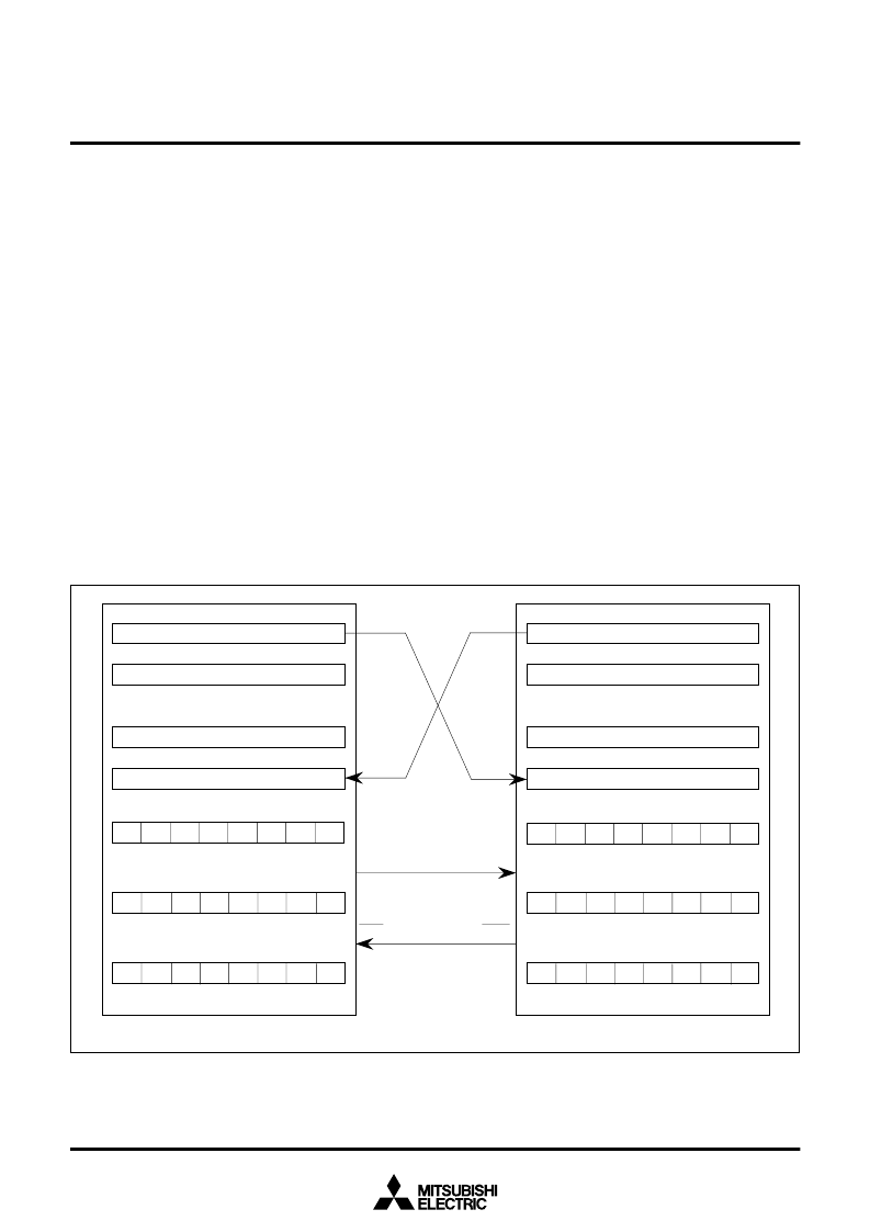
CLOCK SYNCHRONOUS SERIAL
COMMUNICATION
A case where communication is performed between two clock
synchronous serial I/O ports as shown in Figure 41 will be described.
(The transmission side will be denoted by subscript
j
and the receiving
side will be denoted by subscript
k
.)
Bit 0 of the UART
j
transmit/receive mode register and UART
k
transmit/
receive mode register must be set to “1”, and bits 1 and 2 must be
“0”. The length of the transmission data is 8 bits.
Bit 3 of the UART
j
transmit/receive mode register of the clock sending
side is cleared to “0” to select the internal clock. Bit 3 of the UART
k
transmit/receive mode register of the clock receiving side is set to “1”
to select the external clock. Bits 4, 5 and 6 are ignored in the clock
synchronous mode. Bit 7 must always be “0”.
The clock source is selected by bit 0 (CS
0
) and bit 1 (CS
1
) of the
clock sending side UART
j
transmit/receive control register 0. When
the contents of the bit rate genarator is n, as shown in Figure 36, the
selected clock is divided by (n + 1), then by 2, passed through a
transmission control circuit, and output as transmission clock CLK
j
.
Therefore, when the selected clock is f
i
,
Bit Rate = f
i
/ {(n + 1)
2}
On the clock receiving side, the CS
0
and CS
1
bits are ignored because
an external clock is selected.
The bit 2 of the clock sending side UART
j
transmit/receive control
register 0 is cleared to “0” to select
CTS
j
input. The bit 2 of the clock
receiving side is set to “1” to select
k
output.
___
Whether to use signals
CTS
and
RTS
is determined by bit 4 of the
UART transmit/receive control register 0. Set bit 4 to “0” when
CTS
and
RTS
signals are used, and to “1” when they are not used.
UART2 has the
CTS
input function, but that does not have the
RTS
output function (refer to Figure 40.)
When signals
CTS
and
RTS
are not used, the
CTS
/
RTS
pin can be
___
___
and
RTS
are used. When signals
CTS
and
RTS
are not used, the
___
CTS
j
input condition is unnecessary and there is no
RTS
k
output.
Output driver format of the transmit data output pin (T
X
D
j
), which is
the CMOS output or the N-channel open-drain output, is selected
with bit 5 (T
X
S) of the UART
j
transmit/receive control register 0. When
bit 5 is “0”, the CMOS output format is selected. When bit 5 is “1”, the
N-channel open-drain output format is selected. When the N-channel
open-drain output format is selected, make sure to pull-up the data
line using a pull-up resistor.
___
___ ___
___
___
Fig. 41 Clock synchronous serial communication
UART
j
transmission register
UART
j
transmission buffer register
UART
j
receive buffer register
UART
j
receive register
RI
PER
SUM
FER OER
RE
TI
TE
TxD
j
TxD
k
RxD
j
RxD
k
CLK
j
CLK
k
CTS
j
RTS
k
0
0
0
0
1
UART
j
transmit/receive mode register
0
TFM CPL TxS
Tx
EPTY
0
CS
1
CS
0
UART
j
transmit/receive control register 0
UART
j
transmit/receive control register 1
UART
k
transmission register
UART
k
transmission buffer register
UART
k
receive buffer register
UART
k
receive register
TFM CPL TxS
Tx
EPTY
0
1
FER
RI
PER
SUM
OER
RE
TI
TE
UART
k
transmit/receive control register 0
UART
k
transmit/receive control register 1
1
0
0
0
1
UART
k
transmit/receive mode register
___
Note.
UART2 does not include
RTS
output. The UART2 transmit/receive control register 0’s bit configuration is partialy different.
相關(guān)PDF資料 |
PDF描述 |
|---|---|
| M37736MHLXXXHP | SINGLE-CHIP 16-BIT CMOS MICROCOMPUTER |
| M37736EHBXXXGP | PROM VERSION OF M37736MHBXXXGP(MICROCOMPUTERS) |
| M37736MHBXXXGP | SINGLE-CHIP 16-BIT CMOS MICROCOMPUTER |
| M37753FFCFP | SINGLE CHIP 16 BIT CMOS MICROCOMPUTER FLASH MEMORY VERSION |
| M37753FFCHP | SINGLE CHIP 16 BIT CMOS MICROCOMPUTER FLASH MEMORY VERSION |
相關(guān)代理商/技術(shù)參數(shù) |
參數(shù)描述 |
|---|---|
| M37736M4B | 制造商:MITSUBISHI 制造商全稱:Mitsubishi Electric Semiconductor 功能描述:SINGLE-CHIP 16-BIT CMOS MICROCOMPUTER |
| M37736M4BXXXGP | 制造商:MITSUBISHI 制造商全稱:Mitsubishi Electric Semiconductor 功能描述:SINGLE-CHIP 16-BIT CMOS MICROCOMPUTER |
| M37736M4L | 制造商:MITSUBISHI 制造商全稱:Mitsubishi Electric Semiconductor 功能描述:SINGLE-CHIP 16-BIT CMOS MICROCOMPUTER |
| M37736M4LXXXHP | 制造商:MITSUBISHI 制造商全稱:Mitsubishi Electric Semiconductor 功能描述:SINGLE-CHIP 16-BIT CMOS MICROCOMPUTER |
| M37736MHB | 制造商:MITSUBISHI 制造商全稱:Mitsubishi Electric Semiconductor 功能描述:SINGLE-CHIP 16-BIT CMOS MICROCOMPUTER |
發(fā)布緊急采購,3分鐘左右您將得到回復(fù)。