- 您現(xiàn)在的位置:買賣IC網(wǎng) > PDF目錄384636 > M37274MA (Mitsubishi Electric Corporation) Single Chip 8 Bits Microcomputer(8位單片機(jī)) PDF資料下載
參數(shù)資料
| 型號: | M37274MA |
| 廠商: | Mitsubishi Electric Corporation |
| 英文描述: | Single Chip 8 Bits Microcomputer(8位單片機(jī)) |
| 中文描述: | 單芯片8位單片機(jī)(8位單片機(jī)) |
| 文件頁數(shù): | 35/131頁 |
| 文件大小: | 2049K |
| 代理商: | M37274MA |
第1頁第2頁第3頁第4頁第5頁第6頁第7頁第8頁第9頁第10頁第11頁第12頁第13頁第14頁第15頁第16頁第17頁第18頁第19頁第20頁第21頁第22頁第23頁第24頁第25頁第26頁第27頁第28頁第29頁第30頁第31頁第32頁第33頁第34頁當(dāng)前第35頁第36頁第37頁第38頁第39頁第40頁第41頁第42頁第43頁第44頁第45頁第46頁第47頁第48頁第49頁第50頁第51頁第52頁第53頁第54頁第55頁第56頁第57頁第58頁第59頁第60頁第61頁第62頁第63頁第64頁第65頁第66頁第67頁第68頁第69頁第70頁第71頁第72頁第73頁第74頁第75頁第76頁第77頁第78頁第79頁第80頁第81頁第82頁第83頁第84頁第85頁第86頁第87頁第88頁第89頁第90頁第91頁第92頁第93頁第94頁第95頁第96頁第97頁第98頁第99頁第100頁第101頁第102頁第103頁第104頁第105頁第106頁第107頁第108頁第109頁第110頁第111頁第112頁第113頁第114頁第115頁第116頁第117頁第118頁第119頁第120頁第121頁第122頁第123頁第124頁第125頁第126頁第127頁第128頁第129頁第130頁第131頁
35
SINGLE-CHIP 8-BIT CMOS MICROCOMPUTER with CLOSED CAPTION DECODER
and ON-SCREEN DISPLAY CONTROLLER
M37274MA-XXXSP
PRELIMINARY
Notice: This is not a final specification.
Some paramentic limits are subject to change.
MITSUBISHI MICROCOMPUTERS
(1) Clamping Circuit and Low-pass Filter
This filter attenuates the noise of the composite video signal input
from the CV
IN
pin. The CV
IN
pin to which composite video signal is
input requires a capacitor (0.1 μF) coupling outside. Pull down the
CV
IN
pin with a resistor of hundreds of kiloohms to 1 M . In addition,
we recommend to install externally a simple low-pass filter using a
resistor and a capacitor at the CV
IN
pin (refer to Figure 25).
(2) Sync Slice Circuit
This circuit takes out a composite sync signal from the output signal
of the low-pass filter. Figure 27 shows the structure of the sync slice
register.
(3) Synchronous Signal Separation Circuit
This circuit separates a horizontal synchronous signal and a vertical
synchronous signal from the composite sync signal taken out in the
sync slice circuit.
Horizontal synchronous signal (H
sep
)
A one-shot horizontal synchronous signal Hsep is generated at
the falling edge of the composite sync signal.
Vertical synchronous signal (V
sep
)
As a V
sep
signal generating method, it is possible to select one of
the following 2 methods by using bit 7 of the sync slice register
(address 00E3
16
).
Method 1
The “L” level width of the composite sync signal is
measured. If this width exceeds a certain time, a V
sep
signal is generated in synchronization with the rising
of the timing signal immediately after this “L” level.
Method 2
The “L” level width of the composite sync signal is
measured. If this width exceeds a certain time, it is
detected whether a falling of the composite sync
signal exits or not in the “L” level period of the timing
signal immediately after this “L” level. If a falling exists,
a V
sep
signal is generated in synchronization with
the rising of the timing signal (refer to Figure 28).
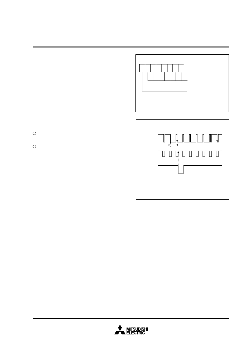
Figure 28 shows a V
sep
generating timing. The timing signal shown
in the figure is generated from the reference clock which the timing
generating circuit outputs.
Reading bit 5 of data slicer control register 2 permits determinating
the shape of the V-pulse portion of the composite sync signal. As
shown in Figure 29, when the A level matches the B level, this bit is
“0.” In the case of a mismatch, the bit is “1.”
For the pins RVCO and the HLF, connect a resistor and a capacitor
as shown in Figure 25. Make the length of wiring which is connected
to these pins as short as possible so that a leakage current may not
be generated.
Note:
It takes a few tens of milliseconds until the reference clock
becomes stable after the data slicer and the timing signal
generating circuit are started. In this period, various timing
signals, H
sep
signals and V
sep
signals become unstable. For
this reason, take stabilization time into consideration when
programming.
Fig. 27. Sync Slice Register
Fig. 28. Vsep Generating Timing (method 2)
0
0
0
0
7
Sync slice register
(SSL : address 00E3
16
)
Fix these bits to “0000101
2
”
Vertical synchronizing
signal (V
sep
) generating
method selection bit
0 : Method 1
1 : Method 2
0
0
1
1
Composite
sync signal
Timing
signal
V
sep
signal
A V
sep
signal is generated at a rising of the timing signal
immediately after the “L” level width of the composite
sync signal exceeds a certain time.
1
2
Measure “L” period
相關(guān)PDF資料 |
PDF描述 |
|---|---|
| M374S1723ETS-C7A | SDRAM Unbuffered Module |
| M366S3323ETS-C7A | SDRAM Unbuffered Module |
| M366S3323ETU-C7A | SDRAM Unbuffered Module |
| M374S1723ETU-C7A | SDRAM Unbuffered Module |
| M374S3323ETS-C7A | SDRAM Unbuffered Module |
相關(guān)代理商/技術(shù)參數(shù) |
參數(shù)描述 |
|---|---|
| M37274MA-052SP | 制造商:MITSUBISHI 制造商全稱:Mitsubishi Electric Semiconductor 功能描述:SINGLE-CHIP 8-BIT CMOS MICROCOMPUTER with CLOSED CAPTION DECODER and ON-SCREEN DISPLAY CONTROLLER |
| M37274MA-053SP | 制造商:MITSUBISHI 制造商全稱:Mitsubishi Electric Semiconductor 功能描述:SINGLE-CHIP 8-BIT CMOS MICROCOMPUTER with CLOSED CAPTION DECODER and ON-SCREEN DISPLAY CONTROLLER |
| M37274MA-082SP | 制造商:MITSUBISHI 制造商全稱:Mitsubishi Electric Semiconductor 功能描述:SINGLE-CHIP 8-BIT CMOS MICROCOMPUTER with CLOSED CAPTION DECODER and ON-SCREEN DISPLAY CONTROLLER |
| M37274MA-084SP | 制造商:MITSUBISHI 制造商全稱:Mitsubishi Electric Semiconductor 功能描述:SINGLE-CHIP 8-BIT CMOS MICROCOMPUTER with CLOSED CAPTION DECODER and ON-SCREEN DISPLAY CONTROLLER |
| M37274MA-XXXSP | 制造商:RENESAS 制造商全稱:Renesas Technology Corp 功能描述:SINGLE-CHIP 8-BIT CMOS MICROCOMPUTER with CLOSED CAPTION DECODER and ON-SCREEN DISPLAY CONTROLLER |
發(fā)布緊急采購,3分鐘左右您將得到回復(fù)。