- 您現(xiàn)在的位置:買賣IC網(wǎng) > PDF目錄180109 > M25PE40VMW6G (STMICROELECTRONICS) 512K X 8 SPI BUS SERIAL EEPROM, PDSO8 PDF資料下載
參數(shù)資料
| 型號: | M25PE40VMW6G |
| 廠商: | STMICROELECTRONICS |
| 元件分類: | PROM |
| 英文描述: | 512K X 8 SPI BUS SERIAL EEPROM, PDSO8 |
| 封裝: | 0.208 INCH, ROHS COMPLIANT, PLASTIC, SOP-8 |
| 文件頁數(shù): | 46/62頁 |
| 文件大小: | 565K |
| 代理商: | M25PE40VMW6G |
第1頁第2頁第3頁第4頁第5頁第6頁第7頁第8頁第9頁第10頁第11頁第12頁第13頁第14頁第15頁第16頁第17頁第18頁第19頁第20頁第21頁第22頁第23頁第24頁第25頁第26頁第27頁第28頁第29頁第30頁第31頁第32頁第33頁第34頁第35頁第36頁第37頁第38頁第39頁第40頁第41頁第42頁第43頁第44頁第45頁當前第46頁第47頁第48頁第49頁第50頁第51頁第52頁第53頁第54頁第55頁第56頁第57頁第58頁第59頁第60頁第61頁第62頁
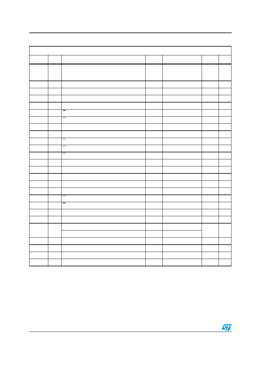
DC and AC parameters
M25PE40
Table 21.
AC characteristics (50 MHz operation, T9HX (0.11m) process(1))(2)
Symbol
Alt.
Parameter
Min.
Typ.
Max.
Unit
fC
Clock frequency for the following instructions:
FAST_READ, RDLR, PW, PP, WRLR, PE, SE,
SSE, DP, RDP, WREN, WRDI, RDSR, WRSR
D.C.
50
MHz
fR
Clock frequency for READ instructions
D.C.
33
MHz
tCH
(3)
tCLH Clock High time
9
ns
tCL
tCLL
Clock Low time
9
ns
Clock Slew Rate (peak to peak)
0.1
V/ns
tSLCH
tCSS S Active Setup time (relative to C)
5
ns
tCHSL
S Not Active Hold time (relative to C)
5
ns
tDVCH
tDSU Data In Setup time
2
ns
tCHDX
tDH
Data In Hold time
5
ns
tCHSH
S Active Hold time (relative to C)
5
ns
tSHCH
S Not Active Setup time (relative to C)
5
ns
tSHSL
tCSH S Deselect time
100
ns
tSHQZ
(4)
tDIS
Output Disable time
8
ns
tCLQV
tV
Clock Low to Output Valid under 30 pF/10 pF
8/6
ns
tCLQX
tHO
Output Hold time
0
ns
tWHSL
(5)
Write Protect Setup time
50
ns
tSHWL
Write Protect Hold time
100
ns
tDP
S to Deep Power-down
3
s
tRDP
S High to Standby mode
30
s
tW
Write Status Register cycle time
3
15
ms
tPW
(6)
Page Write cycle time (256 bytes)
11
23
ms
tPP
Page Program cycle time (256 bytes)
0.8
3ms
Page Program cycle time (n bytes)
int(n/8) × 0.025(7)
tPE
Page Erase cycle time
10
20
ms
tSE
Sector Erase cycle time
1.5
5
s
tSSE
Subsector Erase cycle time
80
150
ms
tBE
Bulk Erase cycle time
8
10
s
1.
2.
Details of how to find the technology process in the marking are given in AN1995, see also Section 13: Ordering
3.
tCH + tCL must be greater than or equal to 1/ fC.
4.
Value guaranteed by characterization, not 100% tested in production.
5.
Only applicable as a constraint for a WRSR instruction when SRWD is set to ‘1’.
6.
When using PP and PW instructions to update consecutive bytes, optimized timings are obtained with one sequence
including all the bytes versus several sequences of only a few bytes (1
≤ n ≤ 256).
7.
int(A) corresponds to the upper integer part of A. For instance, int(12/8) = 2, int(32/8) = 4 int(15.3) =16.
相關(guān)PDF資料 |
PDF描述 |
|---|---|
| M27C1024-10F1X | 1 Mbit 64Kb x16 UV EPROM and OTP EPROM |
| M27C1024-10F3TR | 1 Mbit 64Kb x16 UV EPROM and OTP EPROM |
| M27C1024-10F3X | 1 Mbit 64Kb x16 UV EPROM and OTP EPROM |
| M27C1024-10F6TR | 1 Mbit 64Kb x16 UV EPROM and OTP EPROM |
| M27C1024-10F6X | 1 Mbit 64Kb x16 UV EPROM and OTP EPROM |
相關(guān)代理商/技術(shù)參數(shù) |
參數(shù)描述 |
|---|---|
| M25PE40-VMW6G | 功能描述:閃存 4 Mbit Lo Vltg Page Erasable Seral 閃存 RoHS:否 制造商:ON Semiconductor 數(shù)據(jù)總線寬度:1 bit 存儲類型:Flash 存儲容量:2 MB 結(jié)構(gòu):256 K x 8 定時類型: 接口類型:SPI 訪問時間: 電源電壓-最大:3.6 V 電源電壓-最小:2.3 V 最大工作電流:15 mA 工作溫度:- 40 C to + 85 C 安裝風格:SMD/SMT 封裝 / 箱體: 封裝:Reel |
| M25PE40-VMW6G_NUD | 制造商:Micron Technology Inc 功能描述: |
| M25PE40VMW6P | 制造商:STMICROELECTRONICS 制造商全稱:STMicroelectronics 功能描述:4 Mbit, low voltage, Page-Erasable Serial Flash memory with byte alterability, 50 MHz SPI bus, standard pinout |
| M25PE40-VMW6P | 制造商:NUMONYX 制造商全稱:Numonyx B.V 功能描述:4 Mbit, page-erasable serial Flash memory with byte alterability, 75 MHz SPI bus, standard pinout |
| M25PE40VMW6TG | 制造商:STMICROELECTRONICS 制造商全稱:STMicroelectronics 功能描述:4 Mbit, low voltage, Page-Erasable Serial Flash memory with byte alterability, 50 MHz SPI bus, standard pinout |
發(fā)布緊急采購,3分鐘左右您將得到回復(fù)。