- 您現(xiàn)在的位置:買賣IC網(wǎng) > PDF目錄385472 > LH7A400N0F076B5 (NXP Semiconductors N.V.) 32-Bit System-on-Chip PDF資料下載
參數(shù)資料
| 型號(hào): | LH7A400N0F076B5 |
| 廠商: | NXP Semiconductors N.V. |
| 元件分類: | 數(shù)學(xué)處理器 |
| 英文描述: | 32-Bit System-on-Chip |
| 封裝: | LH7A400N0F000B5<SOT1020-1 (LFBGA256)|<<http://www.nxp.com/packages/SOT1020-1.html<1<Always Pb-free,;LH7A400N0F076B5<SOT1020-1 (LFBGA256)|<<http://www.nxp.com/packages/SOT |
| 文件頁數(shù): | 23/65頁 |
| 文件大小: | 834K |
| 代理商: | LH7A400N0F076B5 |
第1頁第2頁第3頁第4頁第5頁第6頁第7頁第8頁第9頁第10頁第11頁第12頁第13頁第14頁第15頁第16頁第17頁第18頁第19頁第20頁第21頁第22頁當(dāng)前第23頁第24頁第25頁第26頁第27頁第28頁第29頁第30頁第31頁第32頁第33頁第34頁第35頁第36頁第37頁第38頁第39頁第40頁第41頁第42頁第43頁第44頁第45頁第46頁第47頁第48頁第49頁第50頁第51頁第52頁第53頁第54頁第55頁第56頁第57頁第58頁第59頁第60頁第61頁第62頁第63頁第64頁第65頁
32-Bit System-on-Chip
LH7A400
Preliminary data sheet
Rev. 01
—
16 July 2007
23
NXP Semiconductors
External Bus Interface
The external bus interface allows the ARM922T,
LCD controller and DMA engine access to an external
memory system. The LCD controller has access to an
internal frame buffer in embedded SRAM and an exten-
sion buffer in Synchronous Memory for large displays.
The processor and DMA engine share the main system
bus, providing access to all external memory devices
and the embedded SRAM frame buffer.
An arbitration unit ensures that control over the
External Bus Interface (EBI) is only granted when an
existing access has been completed. See Figure 7.
Embedded SRAM
The amount of Embedded SRAM contained in the
LH7A400 is 80 kB. This Embedded memory is
designed to be used for storing code, data, or LCD
frame data and to be contiguous with external SDRAM.
The 80 kB is large enough to store a QVGA panel (320
× 240) at 8 bits per pixel, equivalent to 70 kB of informa-
tion.
Containing the frame buffer on chip reduces the
overall power consumed in any application that uses
the LH7A400. Normally, the system has to perform
external accesses to acquire this data. The LCD con-
troller is designed to automatically use an overflow
frame buffer in SDRAM if a larger screen size is
required. This overflow buffer can be located on any
4 kB page boundary in SDRAM, allowing software to
set the MMU (in the LCD controller) page tables such
that the two memory areas appear contiguous. Byte,
Half-Word and Word accesses are permissible.
Asynchronous Memory Controller
The Asynchronous memory controller is incorpo-
rated as part of the memory controller to provide an
interface between the AMBA AHB system bus and
external (off-chip) memory devices.
The Asynchronous Memory Controller provides sup-
port for up to eight independently configurable memory
banks simultaneously. Each memory bank is capable
of supporting:
SRAM
ROM
Flash EPROM
Burst ROM memory.
Each memory bank may use devices using either 8-,
16-, or 32-bit external memory data paths. The memory
controller supports only little-endian operation.
The memory banks can be configured to support:
Non-burst read and write accesses only to high-
speed CMOS static RAM.
Non-burst write accesses, nonburst read accesses
and asynchronous page mode read accesses to
fast-boot block flash memory.
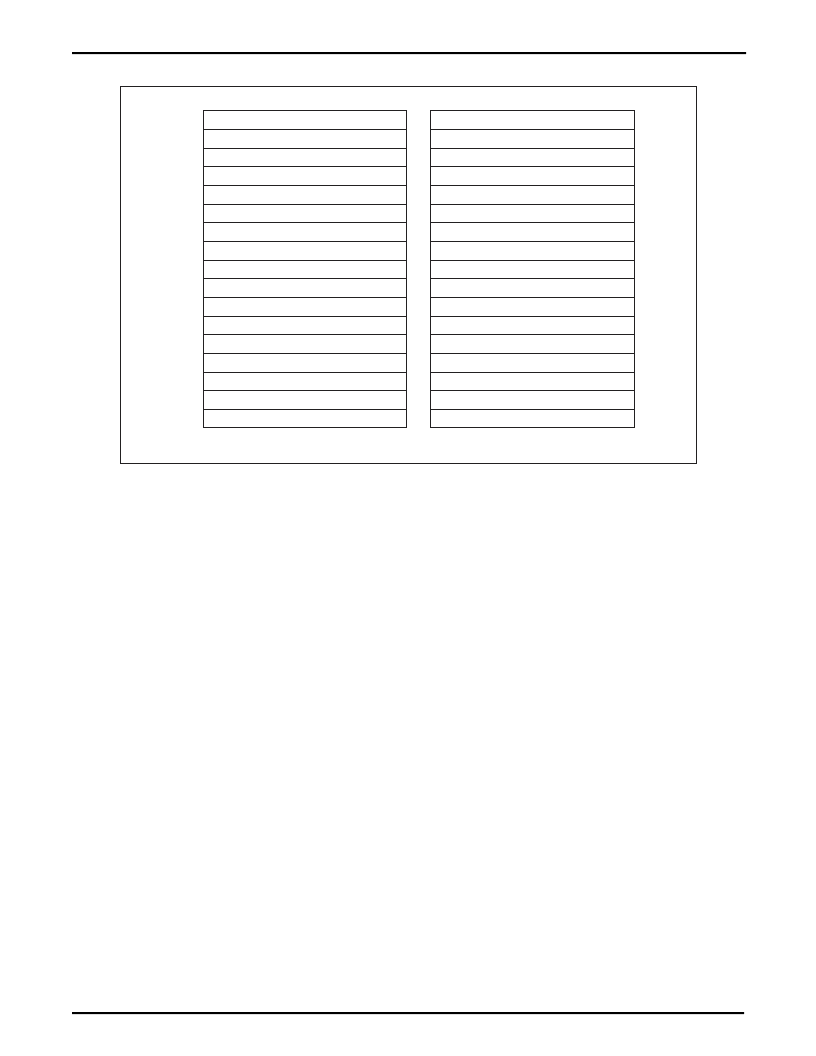
Figure 6. Memory Mapping for Each Boot Mode
ASYNCHRONOUS MEMORY (nCS0)
SYNCHRONOUS MEMORY (nSCS2)
F000.0000
SYNCHRONOUS MEMORY (nSCS1)
D000.0000
SYNCHRONOUS MEMORY (nSCS0)
RESERVED
EMBEDDED SRAM
B001.4000
RESERVED
8000.3800
E000.0000
C000.0000
AHB INTERNAL REGISTERS
APB INTERNAL REGISTERS
8000.0000
ASYNCHRONOUS MEMORY (CS7)
ASYNCHRONOUS MEMORY (CS6)
6000.0000
PCMCIA/CompactFlash (nPCSLOTE2)
PCMCIA/CompactFlash (nPCSLOTE1)
4000.0000
ASYNCHRONOUS MEMORY (nCS3)
ASYNCHRONOUS MEMORY (nCS2)
2000.0000
7000.0000
5000.0000
B000.0000
8000.2000
3000.0000
1000.0000
ASYNCHRONOUS MEMORY (nCS1)
SYNCHRONOUS ROM (nSCS3)
0000.0000
SYNCHRONOUS MEMORY BOOT
SYNCHRONOUS MEMORY (nSCS3)
SYNCHRONOUS MEMORY (nSCS2)
SYNCHRONOUS MEMORY (nSCS1)
SYNCHRONOUS MEMORY (nSCS0)
RESERVED
EMBEDDED SRAM
RESERVED
AHB INTERNAL REGISTERS
APB INTERNAL REGISTERS
ASYNCHRONOUS MEMORY (CS7)
ASYNCHRONOUS MEMORY (CS6)
PCMCIA/CompactFlash (nPCSLOTE2)
PCMCIA/CompactFlash (nPCSLOTE1)
ASYNCHRONOUS MEMORY (nCS3)
ASYNCHRONOUS MEMORY (nCS2)
ASYNCHRONOUS MEMORY (nCS1)
ASYNCHRONOUS ROM (nCS0)
256MB
256MB
256MB
256MB
256MB
256MB
256MB
256MB
256MB
80KB
256MB
256MB
256MB
ASYNCHRONOUS MEMORY BOOT
LH7A400-6
相關(guān)PDF資料 |
PDF描述 |
|---|---|
| LH7A400N0G000B5 | 32-Bit System-on-Chip |
| LH7A404N0F000B3 | 32-Bit System-on-Chip |
| LH7A404N0F092B3 | 32-Bit System-on-Chip |
| LLNRK | LLNRK/LLSRK Series POWR-PRO Class RK1 |
| LLZ4V7 | 500mW Hermetically Sealed Glass Zener Voltage Regulators |
相關(guān)代理商/技術(shù)參數(shù) |
參數(shù)描述 |
|---|---|
| LH7A400N0F076B5,55 | 功能描述:ARM微控制器 - MCU ARM9 LCD USB MMU RoHS:否 制造商:STMicroelectronics 核心:ARM Cortex M4F 處理器系列:STM32F373xx 數(shù)據(jù)總線寬度:32 bit 最大時(shí)鐘頻率:72 MHz 程序存儲(chǔ)器大小:256 KB 數(shù)據(jù) RAM 大小:32 KB 片上 ADC:Yes 工作電源電壓:1.65 V to 3.6 V, 2 V to 3.6 V, 2.2 V to 3.6 V 工作溫度范圍:- 40 C to + 85 C 封裝 / 箱體:LQFP-48 安裝風(fēng)格:SMD/SMT |
| LH7A400N0G000B5 | 功能描述:ARM微控制器 - MCU LCD USB FS/HOST MMU ADC BGA256 RoHS:否 制造商:STMicroelectronics 核心:ARM Cortex M4F 處理器系列:STM32F373xx 數(shù)據(jù)總線寬度:32 bit 最大時(shí)鐘頻率:72 MHz 程序存儲(chǔ)器大小:256 KB 數(shù)據(jù) RAM 大小:32 KB 片上 ADC:Yes 工作電源電壓:1.65 V to 3.6 V, 2 V to 3.6 V, 2.2 V to 3.6 V 工作溫度范圍:- 40 C to + 85 C 封裝 / 箱體:LQFP-48 安裝風(fēng)格:SMD/SMT |
| LH7A400N0G000B5,55 | 功能描述:ARM微控制器 - MCU LCD,USB FS/HOST,MMU,ADC,BGA324 RoHS:否 制造商:STMicroelectronics 核心:ARM Cortex M4F 處理器系列:STM32F373xx 數(shù)據(jù)總線寬度:32 bit 最大時(shí)鐘頻率:72 MHz 程序存儲(chǔ)器大小:256 KB 數(shù)據(jù) RAM 大小:32 KB 片上 ADC:Yes 工作電源電壓:1.65 V to 3.6 V, 2 V to 3.6 V, 2.2 V to 3.6 V 工作溫度范圍:- 40 C to + 85 C 封裝 / 箱體:LQFP-48 安裝風(fēng)格:SMD/SMT |
| LH7A400N0G000B5,551 | 制造商:NXP Semiconductors 功能描述: |
| LH7A400N0G000B5;55 | 功能描述:ARM微控制器 - MCU LCD USB FS/HOST MMU RoHS:否 制造商:STMicroelectronics 核心:ARM Cortex M4F 處理器系列:STM32F373xx 數(shù)據(jù)總線寬度:32 bit 最大時(shí)鐘頻率:72 MHz 程序存儲(chǔ)器大小:256 KB 數(shù)據(jù) RAM 大小:32 KB 片上 ADC:Yes 工作電源電壓:1.65 V to 3.6 V, 2 V to 3.6 V, 2.2 V to 3.6 V 工作溫度范圍:- 40 C to + 85 C 封裝 / 箱體:LQFP-48 安裝風(fēng)格:SMD/SMT |
發(fā)布緊急采購,3分鐘左右您將得到回復(fù)。