- 您現(xiàn)在的位置:買賣IC網(wǎng) > PDF目錄385446 > IRGP50B60PDPBF (International Rectifier) WARP2 SERIES IGBT WITH ULTRAFAST SOFT RECOVERY DIODE PDF資料下載
參數(shù)資料
| 型號(hào): | IRGP50B60PDPBF |
| 廠商: | International Rectifier |
| 英文描述: | WARP2 SERIES IGBT WITH ULTRAFAST SOFT RECOVERY DIODE |
| 中文描述: | WARP2系列IGBT與超快軟恢復(fù)二極管 |
| 文件頁數(shù): | 2/10頁 |
| 文件大小: | 396K |
| 代理商: | IRGP50B60PDPBF |
IRGP50B60PDPbF
2
www.irf.com
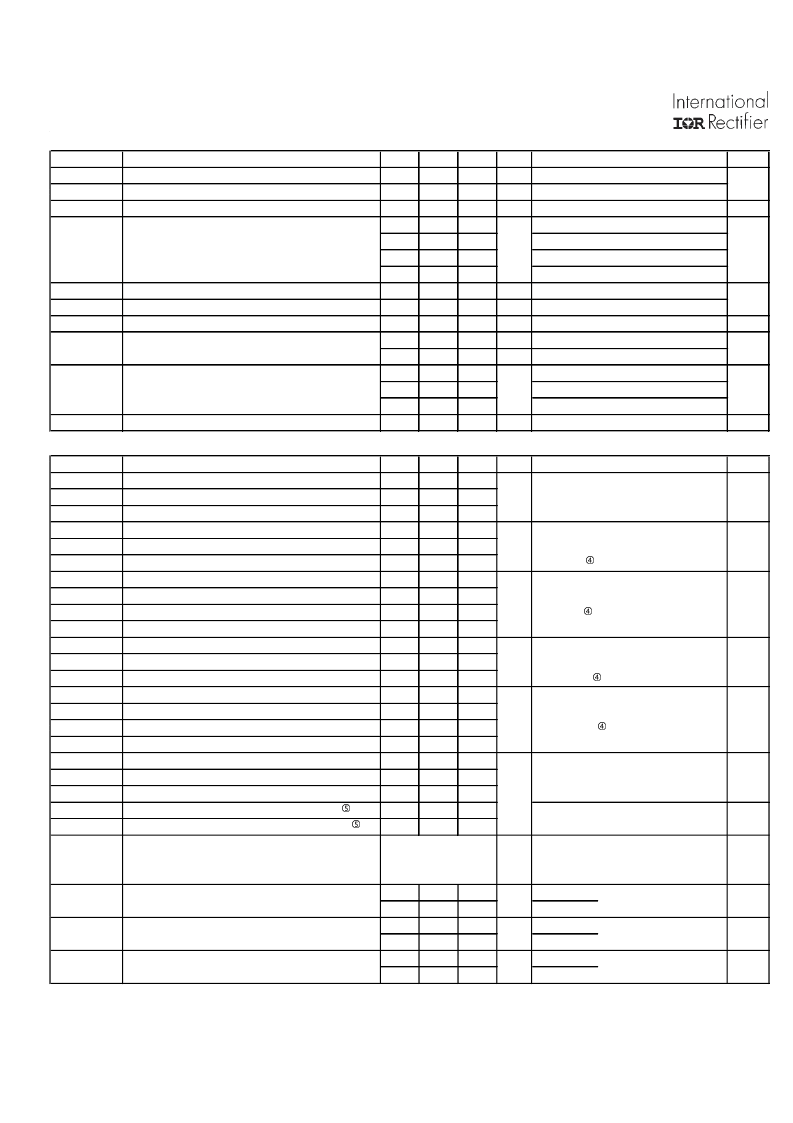
Notes:
R
CE(on)
typ. = equivalent on-resistance = V
CE(on)
typ./ I
C
, where V
CE(on)
typ.= 2.00V and I
C
=33A. I
D
(FET Equivalent) is the equivalent MOSFET I
D
rating @ 25°C for applications up to 150kHz. These are provided for comparison purposes (only) with equivalent MOSFET solutions.
V
CC
= 80% (V
CES
), V
GE
= 20V, L = 28 μH, R
G
= 22
.
Pulse width limited by max. junction temperature.
Energy losses include "tail" and diode reverse recovery, Data generated with use of Diode 30ETH06.
C
oes
eff. is a fixed capacitance that gives the same charging time as C
oes
while V
CE
is rising from 0 to 80% V
CES
.
C
oes
eff.(ER) is a fixed capacitance that stores the same energy as C
oes
while V
CE
is rising from 0 to 80% V
CES
.
Electrical Characteristics @ T
J
= 25°C (unless otherwise specified)
Parameter
V
(BR)CES
Collector-to-Emitter Breakdown Voltage
V
(BR)CES
/
T
J
Temperature Coeff. of Breakdown Voltage
R
G
Internal Gate Resistance
Min.
600
—
—
—
—
—
—
3.0
—
—
—
—
—
—
—
—
Typ.
—
0.61
1.2
2.0
2.4
2.6
3.2
4.0
-7.07
42
5.0
1.0
1.3
1.5
1.3
—
Max. Units Conditions
—
V
V
GE
= 0V, I
C
= 500μA
—
V/°C V
GE
= 0V, I
C
= 1mA (25°C-125°C)
—
1MHz, Open Collector
2.2
I
C
= 33A, V
GE
= 15V
2.6
V
I
C
= 50A, V
GE
= 15V
2.9
I
C
= 33A, V
GE
= 15V, T
J
= 125°C
3.6
I
C
= 50A, V
GE
= 15V, T
J
= 125°C
5.0
V
I
C
= 250μA
—
mV/°C V
CE
= V
GE
, I
C
= 1.0mA
—
S
V
CE
= 50V, I
C
= 33A, PW = 80μs
500
μA
V
GE
= 0V, V
CE
= 600V
—
mA
V
GE
= 0V, V
CE
= 600V, T
J
= 125°C
1.7
I
F
= 25A, V
GE
= 0V
2.0
V
I
F
= 50A, V
GE
= 0V
1.7
I
F
= 25A, V
GE
= 0V, T
J
= 125°C
±100
nA
V
GE
= ±20V, V
CE
= 0V
Ref.Fig
4, 5,6,8,9
V
CE(on)
Collector-to-Emitter Saturation Voltage
V
GE(th)
V
GE(th)
/
TJ
gfe
I
CES
Gate Threshold Voltage
Threshold Voltage temp. coefficient
Forward Transconductance
Collector-to-Emitter Leakage Current
7,8,9
V
FM
Diode Forward Voltage Drop
10
I
GES
Gate-to-Emitter Leakage Current
Switching Characteristics @ T
J
= 25°C (unless otherwise specified)
Parameter
Qg
Total Gate Charge (turn-on)
Q
gc
Gate-to-Collector Charge (turn-on)
Q
ge
Gate-to-Emitter Charge (turn-on)
E
on
Turn-On Switching Loss
E
off
Turn-Off Switching Loss
E
total
Total Switching Loss
t
d(on)
Turn-On delay time
t
r
Rise time
t
d(off)
Turn-Off delay time
t
f
Fall time
E
on
Turn-On Switching Loss
E
off
Turn-Off Switching Loss
E
total
Total Switching Loss
t
d(on)
Turn-On delay time
t
r
Rise time
t
d(off)
Turn-Off delay time
t
f
Fall time
C
ies
Input Capacitance
C
oes
Output Capacitance
C
res
Reverse Transfer Capacitance
C
oes
eff.
Effective Output Capacitance (Time Related)
C
oes
eff. (ER)
Effective Output Capacitance (Energy Related)
Min.
—
—
—
—
—
—
—
—
—
—
—
—
—
—
—
—
—
—
—
—
—
—
Typ.
240
41
84
360
380
740
34
26
130
43
610
460
1070
33
26
140
50
4750
390
58
280
190
Max. Units
360
82
130
590
420
960
44
36
140
56
880
530
1410
43
36
160
65
—
—
—
—
—
Ref.Fig
I
C
= 33A
V
CC
= 400V
V
GE
= 15V
I
C
= 33A, V
CC
= 390V
V
GE
= +15V, R
G
= 3.3
, L = 210μH
TJ = 25°C
I
C
= 33A, V
CC
= 390V
ns
V
GE
= +15V, R
G
= 3.3
, L = 210μH
T
J
= 25°C
17
nC
CT1
CT3
μJ
CT3
I
C
= 33A, V
CC
= 390V
μJ
V
GE
= +15V, R
G
= 3.3
, L = 210μH
T
J
= 125°C
I
C
= 33A, V
CC
= 390V
ns
V
GE
= +15V, R
G
= 3.3
, L = 200μH
T
J
= 125°C
CT3
11,13
WF1,WF2
CT3
12,14
WF1,WF2
V
GE
= 0V
V
CC
= 30V
f = 1Mhz
V
GE
= 0V, V
CE
= 0V to 480V
16
pF
15
T
J
= 150°C, I
C
= 150A
V
CC
= 480V, Vp =600V
Rg = 22
, V
GE
= +15V to 0V
T
J
= 25°C
I
F
= 25A, V
R
= 200V,
T
J
= 125°C
di/dt = 200A/μs
T
J
= 25°C
I
F
= 25A, V
R
= 200V,
T
J
= 125°C
di/dt = 200A/μs
T
J
= 25°C
I
F
= 25A, V
R
= 200V,
T
J
= 125°C
di/dt = 200A/μs
3
RBSOA
Reverse Bias Safe Operating Area
FULL SQUARE
CT2
t
rr
Diode Reverse Recovery Time
—
—
—
—
—
—
50
105
112
420
4.5
8.0
75
160
375
4200
10
15
ns
19
Q
rr
Diode Reverse Recovery Charge
nC
21
I
rr
Peak Reverse Recovery Current
A
19,20,21,22
CT5
Conditions
相關(guān)PDF資料 |
PDF描述 |
|---|---|
| IRGPC20F | Insulated Gate Bipolar Transistors (IGBTs)(快速絕緣柵型雙極型晶體管) |
| IRGPC20M | Insulated Gate Bipolar Transistors (IGBTs)(短路額定超快速絕緣柵型雙極型晶體管) |
| IRGPF20F | Insulated Gate Bipolar Transistors (IGBTs)(快速絕緣柵型雙極型晶體管) |
| IRHF57230SE | RADIATION HARDENED POWER MOSFET THRU-HOLE ( TO-39) |
| IRHM7460SE | TRANSISTOR N-CHANNEL(BVdss=500V, Rds(on)=0.32ohm, Id=18.8A) |
相關(guān)代理商/技術(shù)參數(shù) |
參數(shù)描述 |
|---|---|
| IRGP8B120UD | 制造商:International Rectifier 功能描述:IGBT TRANSISTOR |
| IRGPC20F | 制造商:IRF 制造商全稱:International Rectifier 功能描述:INSULATED GATE BIPOLAR TRANSISTOR(Vces=600V, @Vge=15V, Ic=9.0A) |
| IRGPC20K | 制造商:IRF 制造商全稱:International Rectifier 功能描述:Fit Rate / Equivalent Device Hours |
| IRGPC20KD2 | 制造商:IRF 制造商全稱:International Rectifier 功能描述:Fit Rate / Equivalent Device Hours |
| IRGPC20M | 制造商:IRF 制造商全稱:International Rectifier 功能描述:Fit Rate / Equivalent Device Hours |
發(fā)布緊急采購,3分鐘左右您將得到回復(fù)。