- 您現(xiàn)在的位置:買賣IC網(wǎng) > PDF目錄223993 > HY5PS1G831ALFP-Y5 (HYNIX SEMICONDUCTOR INC) 128M X 8 DDR DRAM, PBGA68 PDF資料下載
參數(shù)資料
| 型號(hào): | HY5PS1G831ALFP-Y5 |
| 廠商: | HYNIX SEMICONDUCTOR INC |
| 元件分類: | DRAM |
| 英文描述: | 128M X 8 DDR DRAM, PBGA68 |
| 封裝: | FBGA-68 |
| 文件頁(yè)數(shù): | 26/36頁(yè) |
| 文件大?。?/td> | 574K |
| 代理商: | HY5PS1G831ALFP-Y5 |
第1頁(yè)第2頁(yè)第3頁(yè)第4頁(yè)第5頁(yè)第6頁(yè)第7頁(yè)第8頁(yè)第9頁(yè)第10頁(yè)第11頁(yè)第12頁(yè)第13頁(yè)第14頁(yè)第15頁(yè)第16頁(yè)第17頁(yè)第18頁(yè)第19頁(yè)第20頁(yè)第21頁(yè)第22頁(yè)第23頁(yè)第24頁(yè)第25頁(yè)當(dāng)前第26頁(yè)第27頁(yè)第28頁(yè)第29頁(yè)第30頁(yè)第31頁(yè)第32頁(yè)第33頁(yè)第34頁(yè)第35頁(yè)第36頁(yè)
Rev. 0.7 / Oct. 2007
32
HY5PS1G431A(L)FP
HY5PS1G831A(L)FP
HY5PS1G1631A(L)FP
9. tIS and tIH (input setup and hold) derating
1) For all input signals the total tIS(setup time) and tIH(hold) time) required is calculated by adding the
datasheet value to the derating value listed in above Table.
Setup(tIS) nominal slew rate for a rising signal is defined as the slew rate between the last crossing of
VREF(dc) and the first crossing of VIH(ac)min. Setup(tIS) nominal slew rate for a falling signal is defined as
the slew rate between the last crossing of VREF(dc) and the first crossing of VIL(ac)max. If the actual signal is
always earlier than the nominal slew rate for line between shaded ‘VREF(dc) to ac region’, use nominal slew
rate for derating value(see fig a.) If the actual signal is later than the nominal slew rate line anywhere
between shaded ‘VREF(dc) to ac region’, the slew rate of a tangent line to the actual signal from the ac level
to dc level is used for derating value(see Fig b.)
Hold(tIH) nominal slew rate for a rising signal is defined as the slew rate between the last crossing of
VIL(dc)max and the first crossing of VREF(dc). Hold(tIH) nominal slew rate for a falling signal is defined as the
slew rate between the last crossing of VREF(dc). If the actual signal is always later than the nominal slew rate
line between shaded ‘dc to VREF(dc) region’, use nominal slew rate for derating value(see Fig.c) If the actual
signal is earlier than the nominal slew rate line anywhere between shaded ‘dc to VREF(dc) region’, the slew
rate of a tangent line to the actual signal from the dc level to VREF(dc) level is used for derating value(see Fig
d.)
Although for slow rates the total setup time might be negative(i.e. a valid input signal will not have reached
VIH/IL(ac) at the time of the rising clock transition) a valid input signal is still required to complete the transi-
tion and reach VIH/IL(ac).
For slew rates in between the values listed in table, the derating values may obtained by linear interpolation.
These values are typically not subject to production test. They are verified by design and characterization.
△tIS
△tIH
△tIS
△tIH
△tIS
△tIH
Units
Notes
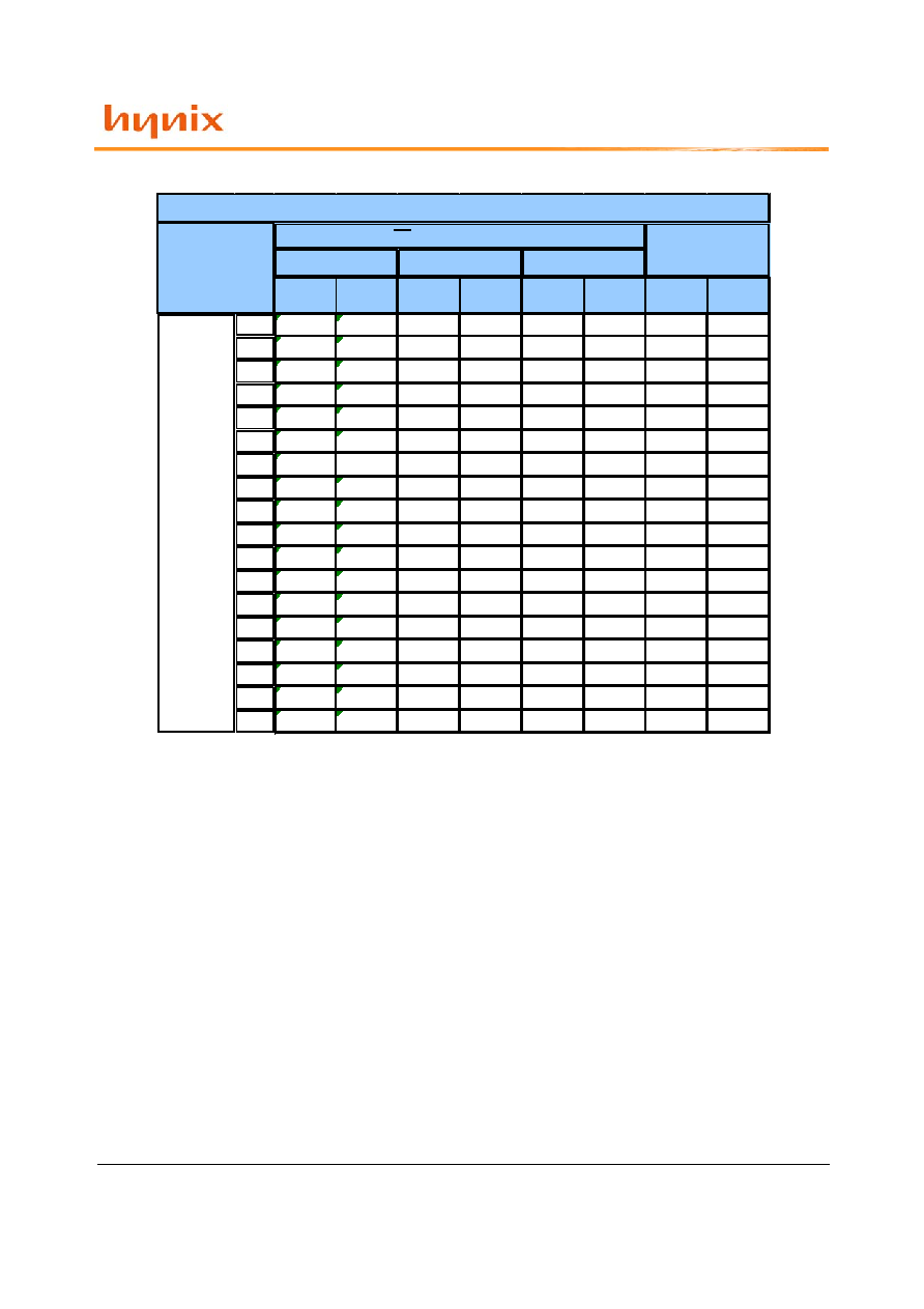
4.0
+187
+94
TBD
ps
1
3.5
+179
+89
TBD
ps
1
3.0
+167
+83
TBD
ps
1
2.5
+150
+75
TBD
ps
1
2.0
+125
+45
TBD
ps
1
1.5
+83
+21
TBD
ps
1
1.0
+0
0
TBDTBD
ps
1
0.9
-11
-14
TBD
ps
1
0.8
-25
-31
TBD
ps
1
0.7
-43
-54
TBD
ps
1
0.6
-67
-83
TBD
ps
1
0.5
-100
-125
TBD
ps
1
0.4
-150
-188
TBD
ps
1
0.3
-223
-292
TBD
ps
1
0.25
-250
-375
TBD
ps
1
0.2
-500
TBD
ps
1
0.15
-750
-708
TBD
ps
1
0.1
-1250
-1125
TBD
ps
1
tIS, tIH Derating Values
Command /
Address
Slew
rate(V/ns)
2.0 V/ns
CK, CK Differential Slew Rate
1.5 V/ns
1.0 V/ns
相關(guān)PDF資料 |
PDF描述 |
|---|---|
| HY5RS573225AFP-16L | 8M X 32 DDR DRAM, 0.28 ns, PBGA136 |
| HY5V28CF-S | 16M X 8 SYNCHRONOUS DRAM, 6 ns, PBGA54 |
| HY5V28CLF-S | 16M X 8 SYNCHRONOUS DRAM, 6 ns, PBGA54 |
| HY5V52CLF-6 | 8M X 32 SYNCHRONOUS DRAM, 5.4 ns, PBGA90 |
| HY5V52EMP-H | 8M X 32 SYNCHRONOUS DRAM, 5.4 ns, PBGA90 |
相關(guān)代理商/技術(shù)參數(shù) |
參數(shù)描述 |
|---|---|
| HY5PS1G831CFP | 制造商:HYNIX 制造商全稱:Hynix Semiconductor 功能描述:1Gb DDR2 SDRAM |
| HY5PS1G831CFP-C4 | 制造商:HYNIX 制造商全稱:Hynix Semiconductor 功能描述:1Gb DDR2 SDRAM |
| HY5PS1G831CFP-E3 | 制造商:HYNIX 制造商全稱:Hynix Semiconductor 功能描述:1Gb DDR2 SDRAM |
| HY5PS1G831CFP-S5 | 制造商:HYNIX 制造商全稱:Hynix Semiconductor 功能描述:1Gb DDR2 SDRAM |
| HY5PS1G831CFP-Y5 | 制造商:HYNIX 制造商全稱:Hynix Semiconductor 功能描述:1Gb DDR2 SDRAM |
發(fā)布緊急采購(gòu),3分鐘左右您將得到回復(fù)。