- 您現(xiàn)在的位置:買賣IC網(wǎng) > PDF目錄375384 > AX88790L (ASIX Electronics Corporation) 10/100BASE 3-in-1 PCMCIA Fast Ethernet Controller PDF資料下載
參數(shù)資料
| 型號: | AX88790L |
| 廠商: | ASIX Electronics Corporation |
| 英文描述: | 10/100BASE 3-in-1 PCMCIA Fast Ethernet Controller |
| 中文描述: | 一個(gè)10/100Base 3合1的PCMCIA快速以太網(wǎng)控制器 |
| 文件頁數(shù): | 11/60頁 |
| 文件大?。?/td> | 633K |
| 代理商: | AX88790L |
第1頁第2頁第3頁第4頁第5頁第6頁第7頁第8頁第9頁第10頁當(dāng)前第11頁第12頁第13頁第14頁第15頁第16頁第17頁第18頁第19頁第20頁第21頁第22頁第23頁第24頁第25頁第26頁第27頁第28頁第29頁第30頁第31頁第32頁第33頁第34頁第35頁第36頁第37頁第38頁第39頁第40頁第41頁第42頁第43頁第44頁第45頁第46頁第47頁第48頁第49頁第50頁第51頁第52頁第53頁第54頁第55頁第56頁第57頁第58頁第59頁第60頁
ASIX ELECTRONICS CORPORATION
11
AX88790 L 3-in-1 PCMCIA Fast Ethernet Controller
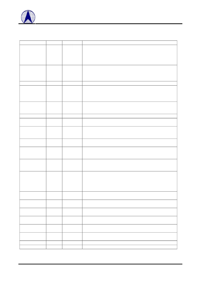
2.8 Miscellaneous pins group
SIGNAL
TYPE
LCLK/XTALIN
I
PIN NO.
79
DESCRIPTION
CMOS Local Clock: Typical a 25Mhz clock, +/- 100 PPM, 40%-60%
duty cycle. The signal not supports 5 Volts tolerance ( See application
note also )
Crystal Oscillator Input: Typical a 25Mhz crystal, +/- 25 PPM can be
connected across XTALIN and XTALOUT.
Crystal Oscillator Output: Typical a 25Mhz crystal, +/- 25 PPM can be
connected across XTALIN and XTALOUT. If a single-ended external
clock (LCLK) is connected to XTALIN, the crystal output pin should
be left floating.
Clock Output: This clock is source from LCLK/XTALIN.
Reset
Reset is active high then place AX88790 into reset mode immediately.
During falling edge the AX88790 loads the power on setting data.
And, after the falling edge the AX88790 loads the EEPROM data.
Test Pins
:
Active high
These pins are just for test mode setting purpose only. Must be pull
down or keep no connection when normal operation.
For test only. Must be pulled down at normal operation.
For test only. Must be pulled down or keep no connection when normal
operation.
FAST_MODE
:
Active LOW
The pin is just for test mode only. Must be pulled high or keep no
connection when normal operation.
EEPROM SIZE = 0: 93C46 type 128 byte EEPROM is used.
EEPROM SIZE = 1: 93C56 type 256 byte EEPROM is used.
This sets the common mode voltage for 10Base-T and 100Base-TX
modes. It should be connected to the center tap of the transmit side of
the transformer
Power Supply: +3.3V DC.
XTALOUT
O
80
CLKO25M
RESET
O
44
3
I/PU
TEST[2:1]
I/PD
47, 65
IDDQ
BIST
I
46
45
I/PD
FAST_MODE#
I/PU
59
EEPROM_SIZE
I/PU
58
ZVREG
O
92
VDD
P
13, 27, 40,
53, 57, 104,
114, 126
14, 28, 34,
43, 52, 54,
63, 64, 94,
105,115,
127
56, 69,
73, 82
55, 68,
72, 75, 85,
76
VSS
P
Power Supply: +0V DC or Ground.
VDDA
P
Power Supply for Analog Circuit: +3.3V DC.
VSSA
P
Power Supply for Analog Circuit: +0V DC or Ground.
VDDM
P
Powers the analog block around the transmit/receive area. This should
be connected to VDDA: +3.3V DC.
Powers the analog block around the transmit/receive area. This should
be connected to VSSA: +0V DC or Ground Power.
The Phase Detector (or PLL) power. This should be isolated with other
power: +3.3V DC.
The Phase Detector (or PLL) power. This should be isolated with other
power: +0V DC or Ground.
Power Supply for Transceiver Output Driver: +3.3V DC.
86, 89, 90 Power Supply for Transceiver Output Driver: +0V DC or Ground.
VSSM
P
77, 93
VDDPD
P
78
VSSPD
P
81
VDDO
VSSO
P
P
91
Tab – 8 Miscellaneous pins group
相關(guān)PDF資料 |
PDF描述 |
|---|---|
| AX88796BLF | IC,MC14411P |
| AX88796BLI | Low-pin-count Non-PCI 8/16-bit 10/100M Fast Ethernet Controller |
| AX88872P | 10/100BASE Dual Speed “Swipeater” Controller |
| AX9902MS | 2N and 2P-Channel Enhancement Mode Power MOSFET |
| AX9902MSA | 2N and 2P-Channel Enhancement Mode Power MOSFET |
相關(guān)代理商/技術(shù)參數(shù) |
參數(shù)描述 |
|---|---|
| AX88796 | 制造商:未知廠家 制造商全稱:未知廠家 功能描述:3-in-1 Local Bus Fast Ethernet Controller |
| AX88796ALF | 制造商:ASIX 功能描述:10/100 MAC,COMMERCIAL 128PIN |
| AX88796BLF | 制造商:Asix Electronics 功能描述:IEEE802.3 / IEEE802.3u LAN standard Ethernet 3.3V 64LQFP Tray 制造商:ASIX 功能描述:10/100 MAC,COMMERCIAL 64PIN |
| AX88796BLI | 制造商:未知廠家 制造商全稱:未知廠家 功能描述:High-Performance Non-PCI Single-Chip 8/16 bit 10/100M Fast Ethernet Controller |
| AX88796C | 制造商:ASIX 制造商全稱:ASIX 功能描述:Low-Power SPI or Non-PCI Ethernet Controller |
發(fā)布緊急采購,3分鐘左右您將得到回復(fù)。