- 您現(xiàn)在的位置:買賣IC網(wǎng) > PDF目錄374035 > ADSP-2173 (Analog Devices, Inc.) DSP Microcomputer(DSP 微計(jì)算機(jī)) PDF資料下載
參數(shù)資料
| 型號(hào): | ADSP-2173 |
| 廠商: | Analog Devices, Inc. |
| 英文描述: | DSP Microcomputer(DSP 微計(jì)算機(jī)) |
| 中文描述: | 微機(jī)的DSP(數(shù)字信號(hào)處理器微計(jì)算機(jī)) |
| 文件頁數(shù): | 31/52頁 |
| 文件大小: | 685K |
| 代理商: | ADSP-2173 |
第1頁第2頁第3頁第4頁第5頁第6頁第7頁第8頁第9頁第10頁第11頁第12頁第13頁第14頁第15頁第16頁第17頁第18頁第19頁第20頁第21頁第22頁第23頁第24頁第25頁第26頁第27頁第28頁第29頁第30頁當(dāng)前第31頁第32頁第33頁第34頁第35頁第36頁第37頁第38頁第39頁第40頁第41頁第42頁第43頁第44頁第45頁第46頁第47頁第48頁第49頁第50頁第51頁第52頁
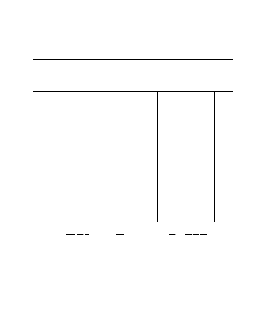
ADSP-2173–SPECIFICATIONS
RECOMMENDEDOPERATINGCONDITIONS
K Grade
Min
B Grade
Min
Parameter
Max
Max
Unit
V
DD
T
AMB
ELECTRICAL CHARACTERISTICS
Supply Voltage
Ambient Operating T emperature
3.0
0
3.6
+70
3.0
–40
3.6
+85
V
°
C
K/B Grades
Min
Parameter
T est Conditions
Max
Unit
V
IH
V
IH
V
IH
V
IL
V
OH
Hi-Level Input Voltage
1, 2
Hi-Level CLK IN Voltage
Hi-Level RESET Voltage
Lo-Level Input Voltage
1, 3
Hi-Level Output Voltage
1, 4, 5
@ V
DD
= max
@ V
DD
= max
@ V
DD
= max
@ V
DD
= min
@ V
DD
= min
I
OH
= –0.5 mA
@ V
DD
= min
I
OH
= –100 mA
6
@ V
DD
= min
I
OL
= 2 mA
@ V
DD
= max
V
IN
= V
DD
max
@ V
DD
= max
V
IN
= 0 V
@ V
DD
= max,
V
IN
= V
DD
max
8
@ V
DD
= max,
V
IN
= 0 V
8
@ V
DD
= max
@ V
DD
= max
t
CK
= 50 ns
11
Lowest Power Mode
12
@ V
IN
= 2.5 V,
f
IN
= 1.0 MHz,
T
AMB
= 25
°
C
@ V
IN
= 2.5 V,
f
IN
= 1.0 MHz,
T
AMB
= 25
°
C
2.0
2.0
2.2
V
V
V
V
0.4
2.4
V
V
DD
– 0.3
V
V
OL
Lo-Level Output Voltage
1, 4, 5
0.4
V
I
IH
Hi-Level Input Current
3
10
μ
A
I
IL
Lo-Level Input Current
3
10
μ
A
I
OZH
T ristate Leakage Current
7
10
μ
A
I
OZL
T ristate Leakage Current
7
10
7
μ
A
mA
I
DD
I
DD
Supply Current (Idle)
9, 10
Supply Current (Dynamic)
10
27
100
mA
μ
A
I
DD
C
I
Supply Current (Powerdown)
10
Input Pin Capacitance
3, 6, 13
8
pF
C
O
Output Pin Capacitance
6, 7, 13, 14
8
pF
NOT ES
Bidirectional pins: D0-D23, RFS0, RFS1, SCLK 0, SCLK 1, T FS0, T FS1, HD0-HD15/HAD0-HAD15.
2
Input only pins:
RESET
,
IRQ2
,
BR
, MMAP, DR0, DR1,
HSEL
, HSIZE, BMODE, HMD0, HMD1,
HRD
/HWR,
HWR
/
HDS
,
PWD
, HA2/ALE, HA1-0.
3
Input only pins: CLK IN,
RESET
,
IRQ2
,
BR
, MMAP, DR0, DR1,
HSEL
, HSIZE, BMODE, HMD0, HMD1,
HRD
/HWR,
HWR
/
HDS
,
PWD
, HA2/ALE, HA1-0.
4
Output pins:
BG
,
PMS
,
DMS
,
BMS
,
RD
,
WR
, PWDACK , A0-A13, DT 0, DT 1, CLK OUT ,
HACK
, FL2-0,
BGH
.
5
Although specified for T T L outputs, all ADSP-2173 outputs are CMOS-compatible and will drive to V
DD
and GND, assuming no dc loads.
6
Guaranteed but not tested.
7
T hree-statable pins: A0-A13, D0-D23,
PMS
,
DMS
,
BMS
,
RD
,
WR
, DT 0, DT 1, SCLK 0, SCLK 1, T FS0, T FS1, RFS0, RSF1, HD0-HD15/HAD0-HAD15.
8
0 V on
BR,
CLK IN Active (to force three-state condition).
9
Idle refers to ADSP-2173 state of operation during execution of IDLE instruction. Deasserted pins are driven to either V
DD
or GND. Current reflects
device operation with CLK OUT disabled.
10
Current reflects device operating with no output loads.
11
V
= 0.4 V and 2.4 V. For typical figures for supply currents, refer to “Power Dissipation” section.
12
See Chapter 9, of the
ADSP-2100 Family User’s Manual
for details.
13
Applies to T QFP and PQFP package types.
14
Output pin capacitance is the capacitve load for any three-state output pin.
Specifications subject to change without notice.
ADSP-2171/ADSP-2172/ADSP-2173
REV. A
–31–
相關(guān)PDF資料 |
PDF描述 |
|---|---|
| ADSP-2181BS-115 | DSP Microcomputer |
| ADSP-2181BS-133 | DSP Microcomputer |
| ADSP-2181KS-115 | DSP Microcomputer |
| ADSP-2181KS-133 | DSP Microcomputer |
| ADSP-2181KS-160 | DSP Microcomputer |
相關(guān)代理商/技術(shù)參數(shù) |
參數(shù)描述 |
|---|---|
| ADSP-2173BS-80 | 制造商:Rochester Electronics LLC 功能描述:- Bulk |
| ADSP-2173BST-80 | 制造商:Analog Devices 功能描述:DSP Fixed-Point 16-Bit 20MHz 20MIPS 128-Pin TQFP 制造商:Rochester Electronics LLC 功能描述:16BIT FXD PT PROC 3.3V - Bulk |
| ADSP-2176-760040 | 制造商:Analog Devices 功能描述: |
| ADSP-2176-760061 | 制造商:Analog Devices 功能描述: |
| ADSP-2176-760243 | 制造商:Analog Devices 功能描述: |
發(fā)布緊急采購(gòu),3分鐘左右您將得到回復(fù)。