- 您現(xiàn)在的位置:買賣IC網(wǎng) > PDF目錄373980 > ADE7758ARW (ANALOG DEVICES INC) Poly Phase Multifunction Energy Metering IC with Per Phase Information PDF資料下載
參數(shù)資料
| 型號: | ADE7758ARW |
| 廠商: | ANALOG DEVICES INC |
| 元件分類: | 模擬信號調(diào)理 |
| 英文描述: | Poly Phase Multifunction Energy Metering IC with Per Phase Information |
| 中文描述: | SPECIALTY ANALOG CIRCUIT, PDSO24 |
| 封裝: | MS-013-AD, SOIC-24 |
| 文件頁數(shù): | 29/68頁 |
| 文件大小: | 1584K |
| 代理商: | ADE7758ARW |
第1頁第2頁第3頁第4頁第5頁第6頁第7頁第8頁第9頁第10頁第11頁第12頁第13頁第14頁第15頁第16頁第17頁第18頁第19頁第20頁第21頁第22頁第23頁第24頁第25頁第26頁第27頁第28頁當前第29頁第30頁第31頁第32頁第33頁第34頁第35頁第36頁第37頁第38頁第39頁第40頁第41頁第42頁第43頁第44頁第45頁第46頁第47頁第48頁第49頁第50頁第51頁第52頁第53頁第54頁第55頁第56頁第57頁第58頁第59頁第60頁第61頁第62頁第63頁第64頁第65頁第66頁第67頁第68頁
ADE7758
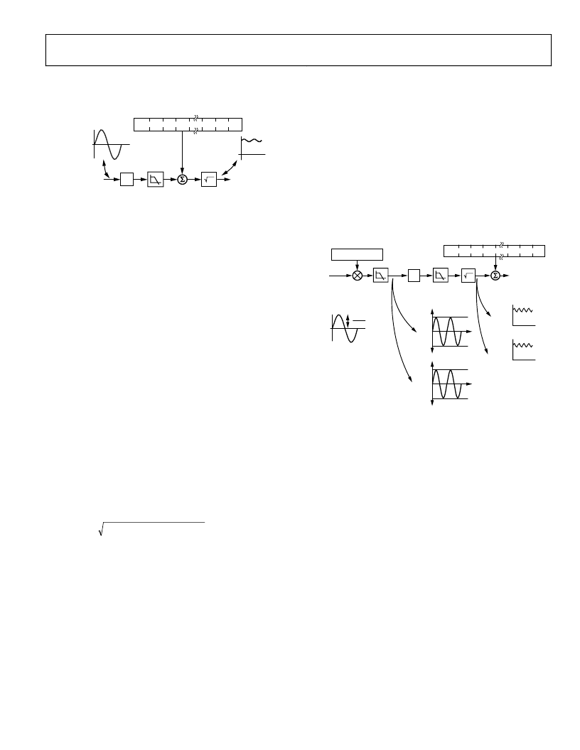
equivalent to one LSB of the current waveform sample. The
update rate of the current rms measurement is CLKIN/12.
Rev. A | Page 29 of 68
0
SGN 2
25
2
24
2
23
2
17
2
16
2
15
CURRENT SIGNAL
FROM HPF OR
INTEGRATOR
(IF ENABLED)
0x1D3781
0x00
+
+
0x2851EC
0x0
0xD7AE14
X
2
LPF3
AIRMS[24:0]
AIRMSOS[11:0]
Figure 62. Current RMS Signal Processing
With the specified full-scale analog input signal of 0.5 V, the
ADC produces an output code that is approximately ±2,642,412d
(see the Current Channel ADC
section). The equivalent rms
values of a full-scale sinusoidal signal at 60 Hz is 1,914,753
(0x1D3781).
The accuracy of the current rms is typically 0.2% error
from the full-scale input down to 1/500 of the full-scale input.
Additionally, this measurement has a bandwidth of 14 kHz.
Current RMS Offset Compensation
The ADE7758 incorporates a current rms offset compensation
for each phase (AIRMSOS, BIRMSOS, and CIRMSOS). These
are 12-bit signed registers that can be used to remove offsets in
the current rms calculations. An offset may exist in the rms
calculation due to input noises that are integrated in the dc
component of I
2
(t). The offset calibration allows the contents of
the IRMS registers to be maintained at 0 when no current is
being consumed. One LSB of the current rms offset register is
equivalent to 16,384 (decimal) of the square of the current rms
register. Assuming that the maximum value from the current
rms calculation is 1,868,467d with full-scale ac inputs, one LSB
of the current rms offset represents 0.94% of the measurement
error at 60 dB down of full scale. For details on how to
calibrate the current rms measurement, see the Calibration
section.
IRMSOS
IRMS
IRMS
0
×
+
=
384
,
16
2
where
IRMS
0
is the rms measurement without offset correction.
Voltage Channel RMS Calculation
Figure 63 shows the details of the signal path for the rms
calculation on Phase A of the voltage channel. The voltage
channel rms value is processed from the waveform samples
after the low-pass filter LPF1. The output of the voltage channel
ADC can be scaled by ±50% by changing VRMSGAIN[11:0]
registers to perform an overall rms voltage calibration. The
VRMSGAIN registers scale the rms calculations as well as the
apparent energy calculation, since apparent power is the
product of the voltage and current rms values. The voltage rms
values are stored in unsigned 24-bit registers (AVRMS, BVRMS,
and CVRMS). The 256 LSBs of the voltage rms register is
approximately equivalent to one LSB of a voltage waveform
sample. The update rate of the voltage rms measurement is
CLKIN
/12.
With the specified full-scale ac analog input signal of 0.5 V, the
LPF1 produces an output code that is approximately 63% of its
full-scale value , i.e., ±9,372d, at 60 Hz (see the Voltage Channel
ADC
section). The equivalent rms value of a full-scale ac signal
is approximately 1,639,101 (0x1902BD) in the VRMS register.
The accuracy of the VRMS measurement is typically 0.5% error
from the full-scale input down to 1/20 of the full-scale input.
Additionally, this measurement has a bandwidth of 160 Hz.
VAN
AVRMSGAIN[11:0]
0x249C
LPF OUTPUT
0x0
60Hz
0xDB64
0x25A2
LPF OUTPUT
WORD RANGE
0x0
50Hz
0xDA5E
LPF1
VOLTAGE SIGNAL–V(t)
0.5
GAIN
0
0x193504
50Hz
0x0
0x1902BD
60Hz
0x0
X
2
AVRMS[23:0]
LPF3
SGN 2
16
2
15
2
14
2
8
2
7
2
6
VRMSOS[11:0]
+
+
Figure 63. Voltage RMS Signal Processing
Voltage RMS Offset Compensation
The ADE7758 incorporates a voltage rms offset compensation
for each phase (AVRMSOS, BVRMSOS, and CVRMSOS).
These are 12-bit signed registers that can be used to remove
offsets in the voltage rms calculations. An offset may exist in the
rms calculation due to input noises and offsets in the input
samples. It should be noted that the offset calibration does not
allow the contents of the VRMS registers to be maintained at 0
when no voltage is applied. This is caused by noise in the
voltage rms calculation, which limits the usable range between
full scale
and 1/50th of full scale. One LSB of the voltage rms offset is
equivalent to 64 LSBs of the voltage rms register.
Assuming that the maximum value from the voltage rms
calculation is 1,639,101d with full-scale ac inputs, then 1 LSB
of the voltage rms offset represents 0.042% of the measurement
error at 1/10 of full scale.
64
×
+
=
VRMSOS
VRMS
VRMS
0
where
VRMS
0
is the rms measurement without the offset
correction.
相關(guān)PDF資料 |
PDF描述 |
|---|---|
| ADE7758ARWRL | Poly Phase Multifunction Energy Metering IC with Per Phase Information |
| ADE7758ARWZ | Poly Phase Multifunction Energy Metering IC with Per Phase Information |
| ADE7758ARWZRL | Poly Phase Multifunction Energy Metering IC with Per Phase Information |
| ADE7759ARSRL | Active Energy Metering IC with di/dt Sensor Interface |
| ADE7759ARS | 8-Channel 14-Bit Single-Supply Voltage-Output DAC; Package: LQFP (10x10mm); No of Pins: 52; Temperature Range: Industrial |
相關(guān)代理商/技術(shù)參數(shù) |
參數(shù)描述 |
|---|---|
| ADE7758ARWRL | 制造商:Analog Devices 功能描述:Energy Measurement 24-Pin SOIC W T/R 制造商:Analog Devices 功能描述:IC ENERGY METER |
| ADE7758ARWZ | 功能描述:IC ENERGY METERING 3PHASE 24SOIC RoHS:是 類別:集成電路 (IC) >> PMIC - 能量測量 系列:- 產(chǎn)品培訓模塊:Lead (SnPb) Finish for COTS Obsolescence Mitigation Program 標準包裝:2,500 系列:* |
| ADE7758ARWZ | 制造商:Analog Devices 功能描述:ENERGY METERING IC 制造商:Analog Devices 功能描述:IC, POLY-PHASE ENERGY METERING, SOIC-24 |
| ADE7758ARWZ | 制造商:Analog Devices 功能描述:IC ENERGY METER 3 PHASE SOIC-24 |
| ADE7758ARWZRL | 功能描述:IC ENERGY METERING 3PHASE 24SOIC RoHS:是 類別:集成電路 (IC) >> PMIC - 能量測量 系列:- 產(chǎn)品培訓模塊:Lead (SnPb) Finish for COTS Obsolescence Mitigation Program 標準包裝:2,500 系列:* |
發(fā)布緊急采購,3分鐘左右您將得到回復。