- 您現(xiàn)在的位置:買賣IC網(wǎng) > PDF目錄373980 > ADE7758ARW (ANALOG DEVICES INC) Poly Phase Multifunction Energy Metering IC with Per Phase Information PDF資料下載
參數(shù)資料
| 型號: | ADE7758ARW |
| 廠商: | ANALOG DEVICES INC |
| 元件分類: | 模擬信號調(diào)理 |
| 英文描述: | Poly Phase Multifunction Energy Metering IC with Per Phase Information |
| 中文描述: | SPECIALTY ANALOG CIRCUIT, PDSO24 |
| 封裝: | MS-013-AD, SOIC-24 |
| 文件頁數(shù): | 20/68頁 |
| 文件大小: | 1584K |
| 代理商: | ADE7758ARW |
第1頁第2頁第3頁第4頁第5頁第6頁第7頁第8頁第9頁第10頁第11頁第12頁第13頁第14頁第15頁第16頁第17頁第18頁第19頁當(dāng)前第20頁第21頁第22頁第23頁第24頁第25頁第26頁第27頁第28頁第29頁第30頁第31頁第32頁第33頁第34頁第35頁第36頁第37頁第38頁第39頁第40頁第41頁第42頁第43頁第44頁第45頁第46頁第47頁第48頁第49頁第50頁第51頁第52頁第53頁第54頁第55頁第56頁第57頁第58頁第59頁第60頁第61頁第62頁第63頁第64頁第65頁第66頁第67頁第68頁
ADE7758
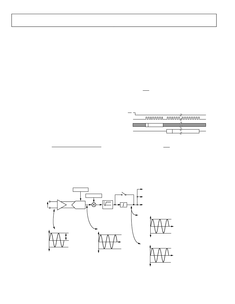
CURRENT CHANNEL ADC
Figure 41 shows the ADC and signal processing path for the
input IA of the current channels (same for IB and IC). In
waveform sampling mode, the ADC outputs are signed twos
complement 24-bit data-words at a maximum of 26.0 kSPS
(thousand samples per second). With the specified full-scale
analog input signal of ±0.5 V, the ADC produces its maximum
output code value (see Figure 41). This diagram shows a full-
scale voltage signal being applied to the differential inputs IAP
and IAN. The ADC output swings between 0xD7AE14
(2,642,412) and 0x2851EC (+2,642,412).
Current Waveform Gain Registers
There is a multiplier in the signal path in the current channel
for each phase. The current waveform can be changed by ±50%
by writing a twos complement number to the 12-bit signed
current waveform gain registers (AIGAIN[11:0], BIGAIN[11:0],
and CIGAIN[11:0]). For example, if 0x7FF is written to those
registers, the ADC output is scaled up by +50%. On the other
hand, writing 0x800 scaled by the output –50%. The expression
below describes mathematically the function of the current
waveform gain registers.
Rev. A | Page 20 of 68
+
×
=
12
2
Register
Gain
Current
of
Content
Output
ADC
Waveform
Current
Changing the content of AIGAIN[11:0], BIGAIN[11:0], or
CIGAIN[11:0] affects all calculations based on its current, i.e., it
affects the phase’s active/reactive/apparent energy as well as its
current rms calculation. In addition, waveform samples are also
scaled accordingly.
Current Channel Sampling
The waveform samples of the current channel can be routed to
the WFORM register at fixed sampling rates by setting the
WAVSEL[2:0] bit in the WAVMODE register to 000 (binary).
The phase in which the samples are routed is set by setting the
PHSEL[1:0] bits in the WAVMODE register. Energy calculation
remains uninterrupted during waveform sampling.
When in waveform sample mode, one of four output sample
rates may be chosen by using Bit 5 and Bit 6 of the WAVMODE
register (DTRT[1:0]). The output sample rate may be 26.0 kSPS,
13.0 kSPS, 6.5 kSPS, or 3.3 kSPS (see Table 16). By setting the
WSMP bit in the interrupt mask register to Logic 1, the interrupt
request output IRQ goes active low when a sample is available.
The timing is shown in Figure 40. The 24-bit waveform samples
are transferred from the ADE7758 one byte (8-bits) at a time,
with the most significant byte shifted out first.
0
READ FROM WAVEFORM
0
12Hex
SGN
CURRENT CHANNEL DATA–24 BITS
SCLK
DIN
DOUT
IRQ
Figure 40. Current Channel Waveform Sampling
The interrupt request output IRQ stays low until the interrupt
routine reads the reset status register (see ADE7758 Interrupts
)
.
0
DIGITAL
INTEGRATOR*
GAIN[7]
ADC
REFERENCE
AIGAIN[11:0]
ACTIVE AND REACTIVE
POWER CALCULATION
WAVEFORM SAMPLE
REGISTER
CURRENT RMS (IRMS)
CALCULATION
IAP
IAN
PGA1
V
IN
GAIN[4:3]
2.42V, 1.21V, 0.6V
GAIN[1:0]
×
1,
×
2,
×
4
ANALOG
INPUT
RANGE
V
IN
0V
0.5V/GAIN
0.25V/GAIN
0.125V/GAIN
ADC OUTPUT
WORD RANGE
CHANNEL 1
(CURRENT WAVEFORM)
DATA RANGE
0xD7AE14
0x000000
0x2851EC
50Hz
CHANNEL 1 (CURRENT WAVEFORM)
DATA RANGE AFTER INTEGRATOR
(50Hz AND AIGAIN[11:0] = 0x000)
0xCB2E48
0x000000
0x34D1B8
60Hz
CHANNEL 1 (CURRENT WAVEFORM)
DATA RANGE AFTER INTEGRATOR
(60Hz AND AIGAIN[11:0] = 0x000)
0xD4176D
0x000000
0x2BE893
HPF
Figure 41. Current Channel Signal Path
相關(guān)PDF資料 |
PDF描述 |
|---|---|
| ADE7758ARWRL | Poly Phase Multifunction Energy Metering IC with Per Phase Information |
| ADE7758ARWZ | Poly Phase Multifunction Energy Metering IC with Per Phase Information |
| ADE7758ARWZRL | Poly Phase Multifunction Energy Metering IC with Per Phase Information |
| ADE7759ARSRL | Active Energy Metering IC with di/dt Sensor Interface |
| ADE7759ARS | 8-Channel 14-Bit Single-Supply Voltage-Output DAC; Package: LQFP (10x10mm); No of Pins: 52; Temperature Range: Industrial |
相關(guān)代理商/技術(shù)參數(shù) |
參數(shù)描述 |
|---|---|
| ADE7758ARWRL | 制造商:Analog Devices 功能描述:Energy Measurement 24-Pin SOIC W T/R 制造商:Analog Devices 功能描述:IC ENERGY METER |
| ADE7758ARWZ | 功能描述:IC ENERGY METERING 3PHASE 24SOIC RoHS:是 類別:集成電路 (IC) >> PMIC - 能量測量 系列:- 產(chǎn)品培訓(xùn)模塊:Lead (SnPb) Finish for COTS Obsolescence Mitigation Program 標(biāo)準(zhǔn)包裝:2,500 系列:* |
| ADE7758ARWZ | 制造商:Analog Devices 功能描述:ENERGY METERING IC 制造商:Analog Devices 功能描述:IC, POLY-PHASE ENERGY METERING, SOIC-24 |
| ADE7758ARWZ | 制造商:Analog Devices 功能描述:IC ENERGY METER 3 PHASE SOIC-24 |
| ADE7758ARWZRL | 功能描述:IC ENERGY METERING 3PHASE 24SOIC RoHS:是 類別:集成電路 (IC) >> PMIC - 能量測量 系列:- 產(chǎn)品培訓(xùn)模塊:Lead (SnPb) Finish for COTS Obsolescence Mitigation Program 標(biāo)準(zhǔn)包裝:2,500 系列:* |
發(fā)布緊急采購,3分鐘左右您將得到回復(fù)。