- 您現(xiàn)在的位置:買賣IC網(wǎng) > PDF目錄373980 > ADE7753ARSRL (ANALOG DEVICES INC) Active and Apparent Energy Metering IC with di/dt sensor interface PDF資料下載
參數(shù)資料
| 型號: | ADE7753ARSRL |
| 廠商: | ANALOG DEVICES INC |
| 元件分類: | 模擬信號調(diào)理 |
| 英文描述: | Active and Apparent Energy Metering IC with di/dt sensor interface |
| 中文描述: | SPECIALTY ANALOG CIRCUIT, PDSO20 |
| 封裝: | MO-150AE, SSOP-20 |
| 文件頁數(shù): | 27/38頁 |
| 文件大小: | 449K |
| 代理商: | ADE7753ARSRL |
第1頁第2頁第3頁第4頁第5頁第6頁第7頁第8頁第9頁第10頁第11頁第12頁第13頁第14頁第15頁第16頁第17頁第18頁第19頁第20頁第21頁第22頁第23頁第24頁第25頁第26頁當(dāng)前第27頁第28頁第29頁第30頁第31頁第32頁第33頁第34頁第35頁第36頁第37頁第38頁
ADE7753
–27–
REV. PrF 10/02
PRELIMINARY TECHNICAL DATA
C L K IN F R E QUE NC Y
In this datasheet, the characteristics of the ADE7753 is shown
with CLK IN frequency equals 3.579545 MHz. However, the
ADE7753 is designed to have the same accuracy at any
CLK IN frequency within the specified range. If the CLK IN
frequency is not 3.579545MHz, various timing and filter
characteristics will need to be redefined with the new CLK IN
frequency. For example, the cut-off frequencies of all digital
filters (LPF1, LPF2, HPF1, etc.) will shift in proportion to
the change in CLK IN frequency according to the following
equation:
MHz
Frequency
579545
CLKIN
.
Frequency
Original
Frequency
New
×
=
(27)
T he change of CLK IN frequency does not affect the timing
characteristics of the serial interface because the data transfer
is synchronized with serial clock signal (SC L K ). But one
needs to observe the read/write timing of the serial data
transfer-see
ADE7753 Timing Characteristics
. T able III lists
various timing changes that are affected by C L K IN fre-
quency.
Table III
Frequency dependencies of the ADE7753 parameters
Parameter
CLKIN dependency
Nyquist frequency for CH 1&2 ADCs
PHCAL resolution (seconds per L SB)
Active Energy register update rate (Hz)
Waveform sampling rate (Number of samples per second)
WAVSEL 1,0 =
0
0
0
1
1
0
1
1
Maximum ZX T OUT period
C L K IN/8
4/C L K IN
C L K IN/4
C L K IN/128
C L K IN/256
C L K IN/512
C L K IN/1024
524,288/C L K IN
SUSPE ND ING T H E A D E 7753 F UNC T IONA L IT Y
T he analog and the digital circuit can be suspended sepa-
rately. T he analog portion of the ADE7753 can be suspended
by setting the ASUSPEND bit (bit 4) of the Mode register
to logic high See
Mode Register
. In suspend mode, all
waveform samples from the ADCs will be set to zeros. T he
digital circuitry can be halted by stopping the CLK IN input
and maintaining a logic high or low on CL K IN pin. T he
ADE7753 can be reactivated by restoring the CLK IN input
and setting the ASUSPEND bit to logic low.
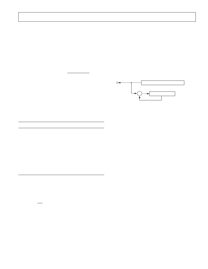
C H E C K SUM R E G IST E R
T he ADE7753 has a Checksum register (CHECK SUM[5:0])
to ensure the data bits received in the last serial read operation
are not corrupted. T he 6-bit C hecksum register is reset
before the first bit (MSB of the register to be read) is put on
the DOUT pin. During a serial read operation, when each
data bit becomes available on the rising edge of SCLK , the
bit will be added to the Checksum register. In the end of the
serial read operation, the content of the Checksum register
will equal to the sum of all ones in the register previously
read. Using the Checksum register, the user can determine
if an error has occured during the last read operation.
Note that a read to the Checksum register will also generate
a checksum of the Checksum register itself.
CHECKSUM REGISTER
CONTENT OF REGISTER (n-bytes)
DOUT
+
+
Σ
ADDR: 3Eh
Figure 48– Checksum register for Serial Interface Read
相關(guān)PDF資料 |
PDF描述 |
|---|---|
| ADE7754 | ADE7754 |
| ADE7754AR | ADE7754 |
| ADE7754ARRL | ADE7754 |
| ADE7755AN-REF | Energy Metering IC with Pulse Output |
| ADE7755ARSRL | Energy Metering IC with Pulse Output |
相關(guān)代理商/技術(shù)參數(shù) |
參數(shù)描述 |
|---|---|
| ADE7753ARSZ | 功能描述:IC ENERGY METERING 1PHASE 20SSOP RoHS:是 類別:集成電路 (IC) >> PMIC - 能量測量 系列:- 產(chǎn)品培訓(xùn)模塊:Lead (SnPb) Finish for COTS Obsolescence Mitigation Program 標(biāo)準(zhǔn)包裝:2,500 系列:* |
| ADE7753ARSZ | 制造商:Analog Devices 功能描述:ENERGY METERING IC |
| ADE7753ARSZ | 制造商:Analog Devices 功能描述:IC MULTIFUNCTION METER |
| ADE7753ARSZRL | 功能描述:IC ENERGY METERING 1PHASE 20SSOP RoHS:是 類別:集成電路 (IC) >> PMIC - 能量測量 系列:- 產(chǎn)品培訓(xùn)模塊:Lead (SnPb) Finish for COTS Obsolescence Mitigation Program 標(biāo)準(zhǔn)包裝:2,500 系列:* |
| ADE7753-ARSZRL | 制造商:Analog Devices 功能描述: |
發(fā)布緊急采購,3分鐘左右您將得到回復(fù)。