- 您現(xiàn)在的位置:買賣IC網(wǎng) > PDF目錄373980 > ADE7753ARSRL (ANALOG DEVICES INC) Active and Apparent Energy Metering IC with di/dt sensor interface PDF資料下載
參數(shù)資料
| 型號: | ADE7753ARSRL |
| 廠商: | ANALOG DEVICES INC |
| 元件分類: | 模擬信號調(diào)理 |
| 英文描述: | Active and Apparent Energy Metering IC with di/dt sensor interface |
| 中文描述: | SPECIALTY ANALOG CIRCUIT, PDSO20 |
| 封裝: | MO-150AE, SSOP-20 |
| 文件頁數(shù): | 15/38頁 |
| 文件大小: | 449K |
| 代理商: | ADE7753ARSRL |
第1頁第2頁第3頁第4頁第5頁第6頁第7頁第8頁第9頁第10頁第11頁第12頁第13頁第14頁當前第15頁第16頁第17頁第18頁第19頁第20頁第21頁第22頁第23頁第24頁第25頁第26頁第27頁第28頁第29頁第30頁第31頁第32頁第33頁第34頁第35頁第36頁第37頁第38頁
ADE7753
–15–
REV. PrF 10/02
PRELIMINARY TECHNICAL DATA
frequency below half the sampling rate. Figure 19 illustrates
the effect. Frequency components (arrows shown in black)
above half the sampling frequency (also know as the Nyquist
frequency, i.e., 447kHz) get imaged or folded back down
below 447kHz (arrows shown in grey). T his will happen with
all ADC s regardless of the architecture. In the example
shown, only frequencies near the sampling frequency, i.e.,
894kHz, will move into the band of interest for metering, i.e,
40Hz - 2kHz. T his allows the usage of very simple LPF (Low
Pass Filter) to attenuate high frequency (near 900kHz) noise
and prevents distortion in the band of interest. For conven-
tional current sensor, a simple RC filter (single pole LPF)
with a corner frequency of 10kHz will produce an attenuation
of approximately 40dBs at 894kHz—see F igure 18. T he
20dB per decade attenuation is usually sufficient to eliminate
the effects of aliasing for conventional current sensor.
For di/dt sensor such as Rogowski coil, however, the sensor
has 20dB per decade gain. T his will neutralize the -20dB per
decade attenuation produced by the simple LPF. T herefore,
when using a di/dt sensor, care should be taken to offset the
20dB per decade gain coming from the di/dt sensor. One
simple approach is to cascade two RC filters to produce the
-40dB per decade attenuation needed.
Frequency (Hz)
Aliasing Effects
0
447kHz
894kHz
2kHz
image
frequencies
Sampling Frequency
Figure 19 —ADC and signal processing in Channel 1
ADC transfer function
Below is an expression which relates the output of the LPF
in the sigma-delta ADC to the analog input signal level. Both
ADCs in the ADE7753 are designed to produce the same
output code for the same input signal level.
V
ADC
Code
144
,
262
0492
.
)
(
×
×
=
out
in
V
T herefore with a full scale signal on the input of 0.5V and an
internal reference of 2.42V, the ADC output code is nomi-
nally 165,151 or 2851Fh. T he maximum code from the
ADC is ±262,144, this is equivalent to an input signal level
of ±0.794V. However for specified performance it is not
recommended that the full-scale input signal level of 0.5V be
exceeded.
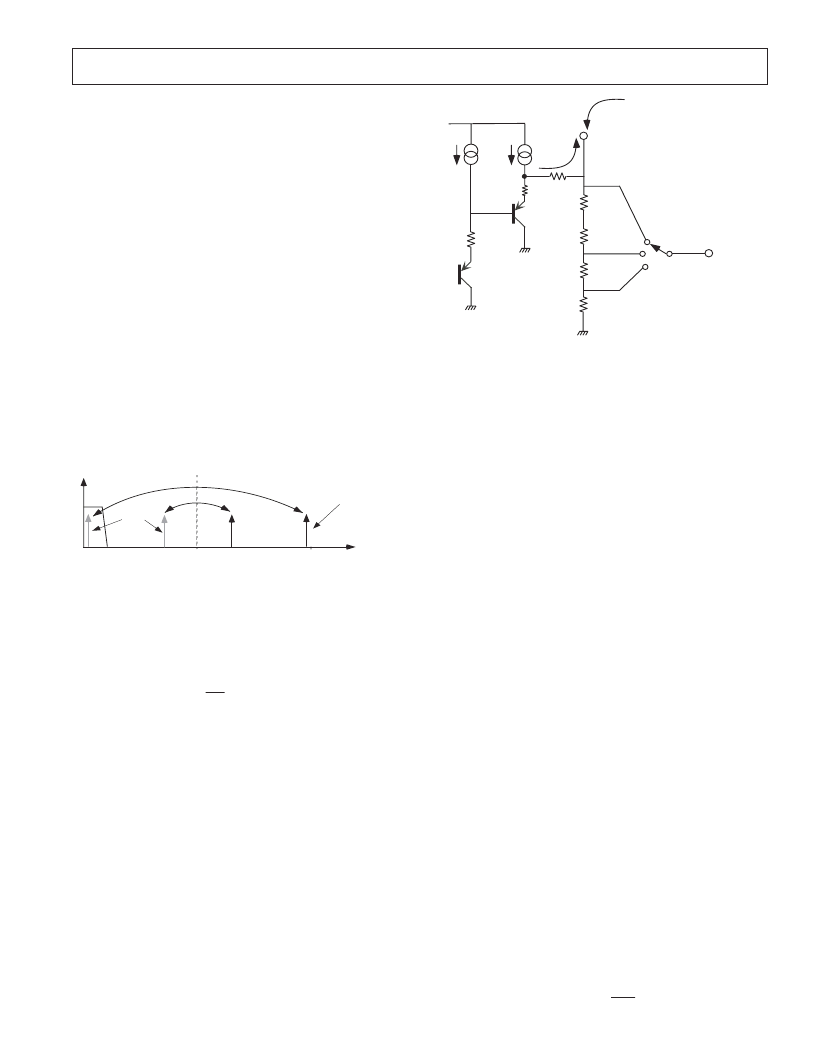
ADE7753 Reference circuit
Shown below in Figure 20 is a simplified version of the
reference output circuitry. T he nominal reference voltage at
the REF
IN/OUT
pin is 2.42V. T his is the reference voltage used
for the ADCs in the ADE7753. However, Channel 1 has
three input range selections which are selected by dividing
down the reference value used for the ADC in Channel 1. T he
reference value used for Channel 1 is divided down to and
of the nominal value by using an internal resistor divider
as shown in Figure 20.
PTAT
60
μ
A
1.7k
12.5k
12.5k
12.5k
12.5k
2.5V
2.42V
REF
IN/OUT
Reference input to ADC
Channel 1 (Range Select)
2.42V, 1.21V, 0.6V
Maximum
Load = 10
μ
A
Output
Impedance
6k
Figure 20 —ADE7753 Reference Circuit Ouput
T he REF
IN/OUT
pin can be overdriven by an external source,
e.g., an external 2.5V reference. Note that the nominal
reference value supplied to the ADCs is now 2.5V not 2.42V.
T his has the effect of increasing the nominal analog input
signal range by 2.5/2.42
×
100% = 3% or from 0.5V to
0.5165V.
T he voltage of AD E 7753 reference drifts slightly with
temperature—see
ADE7753 Specifications
for the temperature
coefficient specification (in ppm/°C ) . T he value of the
temperature drift varies from part to part. Since the reference
is used for the ADCs in both Channel 1 and 2, any
x
% drift
in the reference will result in 2
x
% deviation of the meter
accuracy. T he reference drift resulting from temperature
changes is usually very small and it is typically much smaller
than the drift of other components on a meter. However, if
guaranteed temperature performance is needed, one needs to
use an external voltage reference. Alternatively, the meter can
be calibrated at multiple temperatures. Real time compensa-
tion can be easily achieved using the on the on-chip temperature
sensor.
C HANNE L 1 AD C
Figure 21 shows the ADC and signal processing chain for
Channel 1. In waveform sampling mode the ADC outputs a
signed 2’s Complement 24-bit data word at a maximum of
27.9kSPS (CLK IN/128). With the specified full scale ana-
log input signal of 0.5V (or 0.25V or 0.125V – see
Analog
Inputs
section) the ADC will produce an output code which is
approximately between 2851EC h (+2,642,412 D ecimal)
and D7AE14h (-2,642,412 Decimal). T his is illustrated in
Figure 21.
Channel 1 Sampling
T he waveform samples may also be routed to the WAVE-
FORM register (MODE[14:13] = 1,0) to be read by the
system master (MC U). In waveform sampling mode the
WSMP bit (bit 3) in the Interrupt Enable register must also
be set to logic one. T he Active, Apparent Power and Energy
calculation will remain uninterrupted during waveform sam-
pling.
When in waveform sample mode, one of four output sample
rates may be chosen by using bits 11 and 12 of the Mode
register (WAVSEL 1,0). T he output sample rate may be
27.9kSPS, 14kSPS, 7kSPS or 3.5kSPS—see
Mode Register
.
T he interrupt request output
IRQ
signals a new sample
相關(guān)PDF資料 |
PDF描述 |
|---|---|
| ADE7754 | ADE7754 |
| ADE7754AR | ADE7754 |
| ADE7754ARRL | ADE7754 |
| ADE7755AN-REF | Energy Metering IC with Pulse Output |
| ADE7755ARSRL | Energy Metering IC with Pulse Output |
相關(guān)代理商/技術(shù)參數(shù) |
參數(shù)描述 |
|---|---|
| ADE7753ARSZ | 功能描述:IC ENERGY METERING 1PHASE 20SSOP RoHS:是 類別:集成電路 (IC) >> PMIC - 能量測量 系列:- 產(chǎn)品培訓(xùn)模塊:Lead (SnPb) Finish for COTS Obsolescence Mitigation Program 標準包裝:2,500 系列:* |
| ADE7753ARSZ | 制造商:Analog Devices 功能描述:ENERGY METERING IC |
| ADE7753ARSZ | 制造商:Analog Devices 功能描述:IC MULTIFUNCTION METER |
| ADE7753ARSZRL | 功能描述:IC ENERGY METERING 1PHASE 20SSOP RoHS:是 類別:集成電路 (IC) >> PMIC - 能量測量 系列:- 產(chǎn)品培訓(xùn)模塊:Lead (SnPb) Finish for COTS Obsolescence Mitigation Program 標準包裝:2,500 系列:* |
| ADE7753-ARSZRL | 制造商:Analog Devices 功能描述: |
發(fā)布緊急采購,3分鐘左右您將得到回復(fù)。