- 您現(xiàn)在的位置:買(mǎi)賣(mài)IC網(wǎng) > PDF目錄375252 > ADAV803ASTZ-REEL (ANALOG DEVICES INC) 8-Channel 14-Bit Single-Supply Voltage-Output DAC; Package: LQFP (10x10mm); No of Pins: 52; Temperature Range: Industrial PDF資料下載
參數(shù)資料
| 型號(hào): | ADAV803ASTZ-REEL |
| 廠商: | ANALOG DEVICES INC |
| 元件分類(lèi): | 消費(fèi)家電 |
| 英文描述: | 8-Channel 14-Bit Single-Supply Voltage-Output DAC; Package: LQFP (10x10mm); No of Pins: 52; Temperature Range: Industrial |
| 中文描述: | SPECIALTY CONSUMER CIRCUIT, PQFP64 |
| 封裝: | ROHS COMPLIANT, MS-026BCD, LQFP-64 |
| 文件頁(yè)數(shù): | 15/56頁(yè) |
| 文件大小: | 906K |
| 代理商: | ADAV803ASTZ-REEL |
第1頁(yè)第2頁(yè)第3頁(yè)第4頁(yè)第5頁(yè)第6頁(yè)第7頁(yè)第8頁(yè)第9頁(yè)第10頁(yè)第11頁(yè)第12頁(yè)第13頁(yè)第14頁(yè)當(dāng)前第15頁(yè)第16頁(yè)第17頁(yè)第18頁(yè)第19頁(yè)第20頁(yè)第21頁(yè)第22頁(yè)第23頁(yè)第24頁(yè)第25頁(yè)第26頁(yè)第27頁(yè)第28頁(yè)第29頁(yè)第30頁(yè)第31頁(yè)第32頁(yè)第33頁(yè)第34頁(yè)第35頁(yè)第36頁(yè)第37頁(yè)第38頁(yè)第39頁(yè)第40頁(yè)第41頁(yè)第42頁(yè)第43頁(yè)第44頁(yè)第45頁(yè)第46頁(yè)第47頁(yè)第48頁(yè)第49頁(yè)第50頁(yè)第51頁(yè)第52頁(yè)第53頁(yè)第54頁(yè)第55頁(yè)第56頁(yè)
ADAV803
FUNCTIONAL DESCRIP
ADC SECTION
The ADAV803’s ADC section is implemented using a second-
order multibit (5 bits)
Σ
-
modulator. The modulator is
sampled at either half of the ADC MCLK rate (modulator clo
= 128 × f
S
) or one-quarter of the ADC MCLK rate (modulator
clock = 64 × f
S
). The digital decimator consists of a Sinc^5 filter
followed by a cascade of three half-band FIR filters. The Sin
decimates by a factor of 16 at 48 kHz
96 kHz. Each of the half-band filters decimates by a factor of 2.
Figure 23 shows the details of the ADC section. The ADC can
be clocked by a number of different clock sources to control t
sample rate. MCLK selection for the ADC is set by Internal
Clocking Control Register 1 (Address 0x76). The ADC provide
an output word of up to 24 bits of resolution in twos comple-
ment format. The output word can be routed to ei
output ports, the sample rate converter, or the SPDIF digital
transmitter.
D
S
)
Rev. 0 | Page 15 of 56
TION
ck
c
and by a factor of 8 at
he
s
ther the
P
P
M
X
REG 0x76
BITS 4–2
REG 0x6F
BITS 1–0
0
D
S
)
ADC MCLK
DIVIDER
ADC
MCLK
ADC
Figure 23. Clock Path Control on the ADC
Programmable Gain Amplifier (PGA)
The input of the record channel features a PGA that converts
the single-ended signal to a differential signal, which is applied
to the analog Σ-Δ modulator of the ADC. The PGA can be
programmed to amplify a signal by up to 24 dB in 0.5 dB
increments. Figure 24 shows the structure of the PGA circuit.
4k
TO 64k
125
CAPxN
EXTERNAL
CAPACITOR
(1nF NPO)
VREF
TO
MODULATOR
EXTERNAL
CAPACITOR
(1nF NPO)
CAPxP
EXTERNAL
CAPACITOR
(1nF NPO)
8k
8k
0
4k
125
Figure 24. PGA Block Diagram
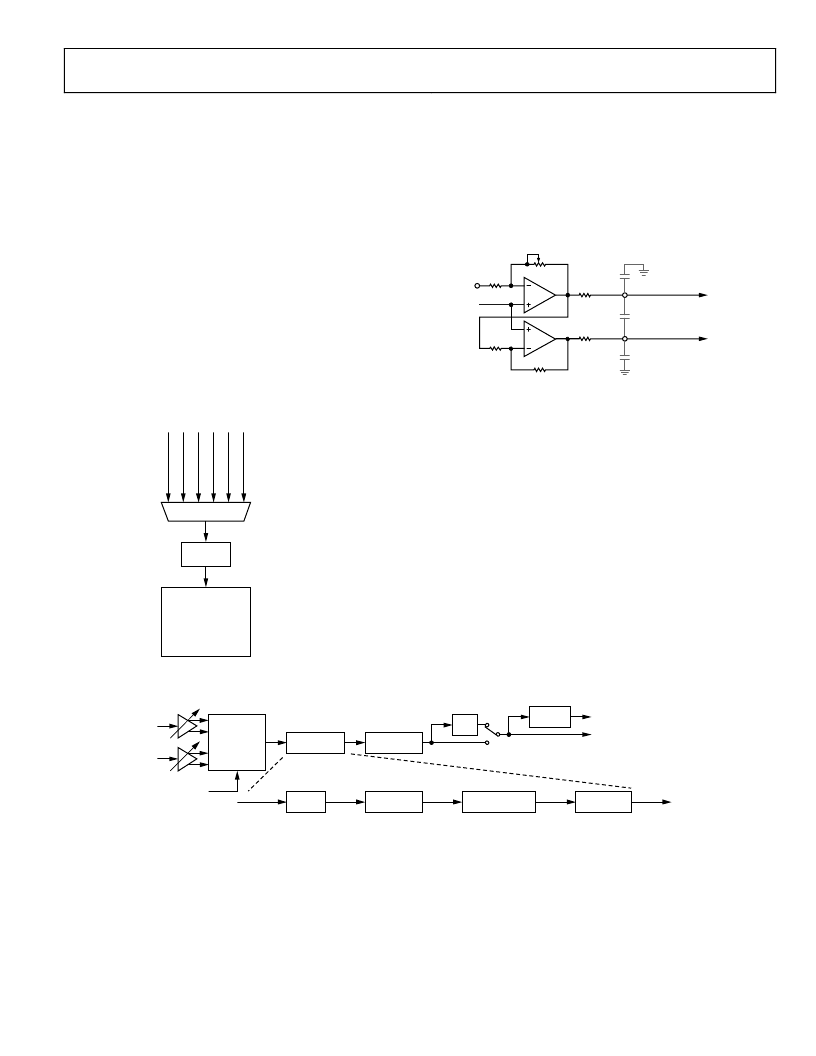
Analog Σ- Modulator
The ADC features a second-order, multibit, Σ-Δ modulator. The
input features two integrators in cascade followed by a flash
converter. This multibit output is directed to a scrambler,
followed by a DAC for loop feedback. The flash ADC output is
also converted from thermometer coding to binary coding for
input as a 5-bit word to the decimator. F
ADC block diagram.
igure 25 shows the
The ADC also features independent digital volume control for
the left and right channels. The volume control consists of
256 linear steps, with each step reducing the digital output
codes by 0.39%. Each channel also has a peak detector that
records the peak level of the input signal. The peak detector
register is cleared by reading it.
ADC MODCLK
MULTI-BIT
Σ
–
MODULATOR
DECIMATOR
HPF
PEAK
DETECT
VOLUME
CONTROL
0
SINC^5
HALF-BAND
FILTER
ADC MCLK/2
(TYP 6.144MHz)
384kHz
768kHz
192k
384k
SINC
COMPENSATION
Hz
Hz
HALF-BAND
FILTER
96kHz
192kHz
48kHz
96kHz
Diagram
Figure 25
. ADC Block
相關(guān)PDF資料 |
PDF描述 |
|---|---|
| ADC-912A | Microprocessor-Compatible 12-Bit A/D Converter(微處理器兼容12位A/D轉(zhuǎn)換器) |
| ADC0834BCN | Serial I/O 8-Bit A/D Converters with Multiplexer Options |
| ADC0834CCN | Serial I/O 8-Bit A/D Converters with Multiplexer Options |
| ADC0838 | Serial I/O 8-Bit A/D Converters with Multiplexer Options |
| ADC0838BCN | Serial I/O 8-Bit A/D Converters with Multiplexer Options |
相關(guān)代理商/技術(shù)參數(shù) |
參數(shù)描述 |
|---|---|
| ADAV804AST | 制造商:Analog Devices 功能描述:AUDIO CODEC FOR RECORDABLE DVD - Bulk |
| ADAV804ASTZ | 制造商:Analog Devices 功能描述: |
| ADB.1X40 | 制造商:FACOM 功能描述:SCREWDRIVER STUB POZI NO.1 制造商:FACOM 功能描述:SCREWDRIVER, STUB, POZI NO.1 制造商:FACOM 功能描述:SCREWDRIVER, STUB, POZI NO.1; Overall Length:90mm; Blade Length:40mm; SVHC:No SVHC (19-Dec-2012); Range:PZ1; Screwdriver Type:Pozi; Tip / Nozzle Size:PZ1; Tip / Nozzle Style:Pozidriv ;RoHS Compliant: NA |
| ADB0039 | 制造商:AVOCENT 功能描述:Cyclades - Crossover adapter - RJ-45 (M) - RJ-45 (F) |
| ADB-1 | 制造商:IDEC CORPORATION 功能描述:LACHING BEAM ATTACH |
發(fā)布緊急采購(gòu),3分鐘左右您將得到回復(fù)。