- 您現(xiàn)在的位置:買賣IC網(wǎng) > PDF目錄375249 > AD9865BCPZRL1 (Analog Devices, Inc.) Broadband Modem Mixed-Signal Front End PDF資料下載
參數(shù)資料
| 型號: | AD9865BCPZRL1 |
| 廠商: | Analog Devices, Inc. |
| 英文描述: | Broadband Modem Mixed-Signal Front End |
| 中文描述: | 寬帶調(diào)制解調(diào)器混合信號前端 |
| 文件頁數(shù): | 40/48頁 |
| 文件大?。?/td> | 1672K |
| 代理商: | AD9865BCPZRL1 |
第1頁第2頁第3頁第4頁第5頁第6頁第7頁第8頁第9頁第10頁第11頁第12頁第13頁第14頁第15頁第16頁第17頁第18頁第19頁第20頁第21頁第22頁第23頁第24頁第25頁第26頁第27頁第28頁第29頁第30頁第31頁第32頁第33頁第34頁第35頁第36頁第37頁第38頁第39頁當(dāng)前第40頁第41頁第42頁第43頁第44頁第45頁第46頁第47頁第48頁
AD9865
occurs within 100 ns. The user-programmable delay for the Tx
path power-down is meant to match the pipeline delay of the
last Tx burst sample such that power-down of the TxDAC and
IAMP does not impact its transmission. A 5-bit field in Register 0x03
sets the delay from 0 to 31 TXCLK clock cycles, with the default
being 31 (0.62 μs with f
TXCLK
= 50 MSPS). The digital interpolation
filter is automatically flushed with midscale samples prior to
power-down, if the clock signal into the TXCLK pin is present
for 33 additional clock cycles after
TXEN returns low. For an Rx
burst, the rising edge of TXEN is used to generate an internal
signal (with no delay) that powers up the Tx circuitry within 0.5 μs.
Rev. A | Page 40 of 48
The Rx path power-on/power-off can be controlled by either
TXEN or RXEN by setting Bit 2 of Register 0x03. In the default
setting, the falling edge of TXEN powers up the Rx circuitry
within 2 μs, while the rising edge of TXEN powers down the Rx
circuitry within 0.5 μs. If RXEN is selected as the control signal,
then its rising edge powers up the Rx circuitry and the falling
edge powers it down. To disable the fast power-down of the Tx
and/or Rx circuitry, set Bit 1 and/or Bit 0 to 0.
POWER REDUCTION OPTIONS
The power consumption of the AD9865 can be significantly
reduced from its default setting by optimizing the power
consumption versus performance of the various functional
blocks in the Tx and Rx signal path. On the Tx path, minimum
power consumption is realized when the TxDAC output is used
directly and its standing current, I, is reduced to as low as 1 mA.
Although a slight degradation in THD performance results at
reduced standing currents, it often remains adequate for most
applications, because the op amp driver typically limits the
overall linearity performance of the Tx path. The load resistors
used at the TxDAC outputs (IOUTP+ and IOUTP) can be
increased to generate an adequate differential voltage that can
be further amplified via a power efficient op-amp-based driver
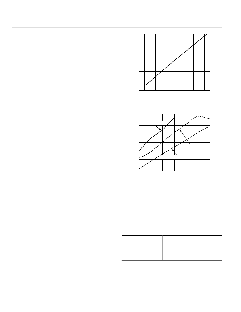
solution. Figure 78 shows how the supply current for the
TxDAC (Pin 43) is reduced from 55 mA to 14 mA as the
standing current is reduced from 12.5mA to 1.25 mA. Further
Tx power savings can be achieved by bypassing or reducing the
interpolation factor of the digital filter as shown in Figure 79.
0
I
STANDING
(mA)
I
T
0
1
2
3
4
5
6
7
8
9
10
11
12
13
55
10
15
20
25
30
35
40
45
50
Figure 78. Reduction in TxDAC’s Supply Current vs. Standing Current
0
INPUT DATA RATE (MSPS)
I
D
20
30
40
50
60
70
80
55
60
65
15
20
25
30
35
40
45
50
2
×
INTERPOLATION
4
×
INTERPOLATION
1
×
(HALF-DUPLEX ONLY)
Figure 79. Digital Supply Current Consumption vs. Input Data Rate
(DVDD = DRVDD =3.3 V and f
OUT
= f
DATA
/10)
Power consumption on the Rx path can be achieved by reduc-
ing the bias levels of the various amplifiers contained within the
RxPGA and ADC. As previously noted, the RxPGA consists of
two CPGA amplifiers and one SPGA amplifier. The bias levels
of each of these amplifiers along with the ADC can be con-
trolled via Register 0x13, as shown in Table 24. The default
setting for 0x13 is 0x00.
Table 24. SPI Register for RxPGA and ADC Biasing
Address (Hex)
0x07
0x13
Bit
(4)
(7:5)
(4:3)
(2:0)
Description
ADC low power
CPGA bias adjust
SPGA bias adjust
ADC power bias adjust
相關(guān)PDF資料 |
PDF描述 |
|---|---|
| AD9865CHIPS | Broadband Modem Mixed-Signal Front End |
| AD9887 | Dual Interface for Flat Panel Displays |
| AD9888 | 100/140/170/205 MSPS Analog Flat Panel Interface |
| AD9888KS-100 | 100/140/170/205 MSPS Analog Flat Panel Interface |
| AD9888KS-140 | TRI N PLUG F 2-13 |
相關(guān)代理商/技術(shù)參數(shù) |
參數(shù)描述 |
|---|---|
| AD9865CHIPS | 制造商:AD 制造商全稱:Analog Devices 功能描述:Broadband Modem Mixed-Signal Front End |
| AD9865-EB | 制造商:Analog Devices 功能描述:MODEM, BROADBAND MODEM MIXED SGNL FRONT END - Bulk |
| AD9866 | 制造商:AD 制造商全稱:Analog Devices 功能描述:Broadband Modem Mixed-Signal Front End |
| AD9866BCP | 制造商:Analog Devices 功能描述:Mixed Signal Front End 64-Pin LFCSP EP 制造商:Analog Devices 功能描述:12BIT MIXED SIGNAL CONVERTER 9866 |
| AD9866BCPRL | 制造商:Analog Devices 功能描述:Mixed Signal Front End 64-Pin LFCSP EP T/R |
發(fā)布緊急采購,3分鐘左右您將得到回復(fù)。