- 您現(xiàn)在的位置:買賣IC網(wǎng) > PDF目錄375249 > AD9865BCPZRL1 (Analog Devices, Inc.) Broadband Modem Mixed-Signal Front End PDF資料下載
參數(shù)資料
| 型號: | AD9865BCPZRL1 |
| 廠商: | Analog Devices, Inc. |
| 英文描述: | Broadband Modem Mixed-Signal Front End |
| 中文描述: | 寬帶調(diào)制解調(diào)器混合信號前端 |
| 文件頁數(shù): | 34/48頁 |
| 文件大小: | 1672K |
| 代理商: | AD9865BCPZRL1 |
第1頁第2頁第3頁第4頁第5頁第6頁第7頁第8頁第9頁第10頁第11頁第12頁第13頁第14頁第15頁第16頁第17頁第18頁第19頁第20頁第21頁第22頁第23頁第24頁第25頁第26頁第27頁第28頁第29頁第30頁第31頁第32頁第33頁當(dāng)前第34頁第35頁第36頁第37頁第38頁第39頁第40頁第41頁第42頁第43頁第44頁第45頁第46頁第47頁第48頁
AD9865
LOW-PASS FILTER
The low-pass filter (LPF) provides a third order response with a
cutoff frequency that is typically programmable over a 15 MHz
to 35 MHz span. Figure 68 shows that the first real pole is im-
plemented within the first CPGA gain stage, and the complex
pole pair is implemented in the second CPGA gain stage.
Capacitor arrays are used to vary the different R-C time con-
stants within these two stages in a manner that changes the
cutoff frequency while preserving the normalized frequency
response. Because absolute resistor and capacitor values are
process-dependent, a calibration routine lasting less than 100 μs
automatically occurs each time the target
cutoff frequency
register (Register 0x08) is updated, ensuring a repeatable cutoff
frequency from device to device.
Rev. A | Page 34 of 48
Although the default setting specifies that the LPF be active, it
can also be bypassed providing a nominal f
3 dB
of 55 MHz.
Table 20 shows the SPI registers pertaining to the LPF.
Table 20. SPI Registers for Rx Low-Pass Filter
Address (Hex)
0x07
0x08
Bit
(0)
(7:0)
Description
Enable Rx LPF
Target
value
The normalized wideband gain response is shown in Figure 70.
The normalized pass-band gain and group delay responses are
shown in Figure 71. The normalized cutoff frequency, f
3 dB
,
results in 3 dB attenuation. Also, the actual group delay time
(GDT) response can be calculated given a programmed cutoff
frequency using the following equation:
Actual GDT = Normalized GDT
/(2.45 ×
f
3dB
)
(7)
4
FREQUENCY
G
0
5
1.0
3.0
–35
–30
–25
–20
–15
–10
–5
0
2.5
2.0
1.5
0.5
Figure 70. LPF’s Normalized Wideband Gain Response
4
NORMALIZED FREQUENCY
G
0
0.5
1.0
0.9
0.3
0.4
0.8
0.2
0.1
N
T
1.30
0.65
0.70
0.75
0.80
0.85
0.90
0.95
1.00
1.05
1.10
1.15
1.20
1.25
0.25
–3.00
–2.75
–2.50
–2.25
–2.00
–1.75
–1.50
–1.25
–1.00
–0.75
–0.50
–0.25
0
0.6
0.7
NORMALIZED GROUP DELAY
NORMALIZED GAIN RESPONSE
Figure 71. LPF’s Normalized Pass-Band Gain and Group Delay Responses
The 3 dB cut-off frequency, f
3 dB
, is programmable by writing
an 8-bit word, referred to as the target,
to Register 0x08. The
cutoff frequency is a function of the ADC sample rate, f
ADC
, and
to a lesser extent, the RxPGA gain setting (in dB). Figure 72
shows how the frequency response, f
3 dB
, varies as a function of
the RxPGA gain setting.
4
INPUT FREQUENCY (MHz)
F
0
10
50
30
25
5
3
–18
–12
–6
0
15
20
35
40
–15
–9
–3
45
–6dB GAIN
0dB GAIN
+6dB GAIN
+18dB GAIN
+30dB GAIN
+42dB GAIN
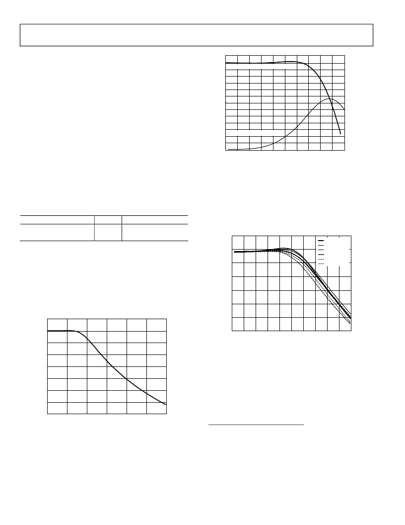
Figure 72. Effects of RxPGA Gain on LPF Frequency Response
(f
3 dB
= 32 MHz (@ 0 dB and f
ADC
= 80 MSPS)
The following formula
1
can be used to estimate f
3 dB
for a
RxPGA gain setting of 0 dB:
f
3dB_0dB
= (128/
target
) × (
f
ADC
/80) ×(
f
ADC
/30 + 23.83)
f
(8)
Figure 73 compares the measured and calculated f
3 dB
using this
formula.
1
Empirically derived for a f
3 dB
range of 15 MHz to 35 MHz and f
ADC
of 40 MSPS
to 80 MSPS with an RxPGA = 0 dB.
相關(guān)PDF資料 |
PDF描述 |
|---|---|
| AD9865CHIPS | Broadband Modem Mixed-Signal Front End |
| AD9887 | Dual Interface for Flat Panel Displays |
| AD9888 | 100/140/170/205 MSPS Analog Flat Panel Interface |
| AD9888KS-100 | 100/140/170/205 MSPS Analog Flat Panel Interface |
| AD9888KS-140 | TRI N PLUG F 2-13 |
相關(guān)代理商/技術(shù)參數(shù) |
參數(shù)描述 |
|---|---|
| AD9865CHIPS | 制造商:AD 制造商全稱:Analog Devices 功能描述:Broadband Modem Mixed-Signal Front End |
| AD9865-EB | 制造商:Analog Devices 功能描述:MODEM, BROADBAND MODEM MIXED SGNL FRONT END - Bulk |
| AD9866 | 制造商:AD 制造商全稱:Analog Devices 功能描述:Broadband Modem Mixed-Signal Front End |
| AD9866BCP | 制造商:Analog Devices 功能描述:Mixed Signal Front End 64-Pin LFCSP EP 制造商:Analog Devices 功能描述:12BIT MIXED SIGNAL CONVERTER 9866 |
| AD9866BCPRL | 制造商:Analog Devices 功能描述:Mixed Signal Front End 64-Pin LFCSP EP T/R |
發(fā)布緊急采購,3分鐘左右您將得到回復(fù)。