- 您現(xiàn)在的位置:買(mǎi)賣(mài)IC網(wǎng) > PDF目錄375249 > AD9865BCPRL (ANALOG DEVICES INC) Broadband Modem Mixed-Signal Front End PDF資料下載
參數(shù)資料
| 型號(hào): | AD9865BCPRL |
| 廠商: | ANALOG DEVICES INC |
| 元件分類(lèi): | 通信及網(wǎng)絡(luò) |
| 英文描述: | Broadband Modem Mixed-Signal Front End |
| 中文描述: | SPECIALTY TELECOM CIRCUIT, QCC64 |
| 封裝: | MO-220-VMMD, LFCSP-64 |
| 文件頁(yè)數(shù): | 22/48頁(yè) |
| 文件大小: | 1672K |
| 代理商: | AD9865BCPRL |
第1頁(yè)第2頁(yè)第3頁(yè)第4頁(yè)第5頁(yè)第6頁(yè)第7頁(yè)第8頁(yè)第9頁(yè)第10頁(yè)第11頁(yè)第12頁(yè)第13頁(yè)第14頁(yè)第15頁(yè)第16頁(yè)第17頁(yè)第18頁(yè)第19頁(yè)第20頁(yè)第21頁(yè)當(dāng)前第22頁(yè)第23頁(yè)第24頁(yè)第25頁(yè)第26頁(yè)第27頁(yè)第28頁(yè)第29頁(yè)第30頁(yè)第31頁(yè)第32頁(yè)第33頁(yè)第34頁(yè)第35頁(yè)第36頁(yè)第37頁(yè)第38頁(yè)第39頁(yè)第40頁(yè)第41頁(yè)第42頁(yè)第43頁(yè)第44頁(yè)第45頁(yè)第46頁(yè)第47頁(yè)第48頁(yè)
AD9865
Rev. A | Page 22 of 48
SCLK
SDATA
SCLK
SDATA
R/W
N1
A1
A2
A3
A4
A0
N2
D71D61
D1N D0N
R/W
N1
A1
A2
A3
A4
A0
N2
D01D11
D7N
D6N
4
DATA TRANSFER CYCLE
INSTRUCTION CYCLE
DATA TRANSFER CYCLE
INSTRUCTION CYCLE
SEN
SEN
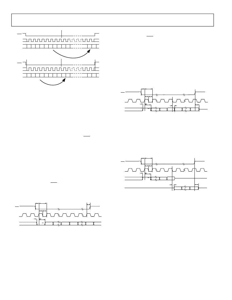
Figure 45. SPI Timing, MSB First (Upper), and LSB First (Lower)
When the SPI LSB first bit is set high, the serial port interprets
both instruction and data bytes LSB first. Multibyte data trans-
fers in LSB format can be completed by writing an instruction
byte that includes the register address of the first
address to be
accessed. The AD9865 automatically increments the address for
each successive byte required for the multibyte communication
cycle.
Figure 46 illustrates the timing requirements for a write opera-
tion to the SPI port. After the serial port enable (SEN) signal
goes low, data (SDIO) pertaining to the instruction header is
read on the rising edges of the clock (SCLK). To initiate a write
operation, the read/not-write bit is set low. After the instruction
header is read, the eight data bits pertaining to the specified
register are shifted into the SDIO pin on the rising edge of the
next eight clock cycles. If a multibyte communication cycle is
specified, the destination address is decremented (MSB first)
and shifts in another eight bits of data. This process repeats until
all the bytes specified in the instruction header (N1, N0 bits) are
shifted into the SDIO pin. SEN must remain low during the data
transfer operation, only going high after the last bit is shifted
into the SDIO pin.
D7
D6
A0
D1
SEN
N1
N0
t
S
SCLK
SDIO
1/
f
SCLK
t
LOW
t
HI
t
DS
t
DH
R/W
D0
t
H
4
Figure 46. SPI Write Operation Timing
Figure 47 illustrates the timing for a 3-wire read operation to
the SPI port. After SEN goes low, data (SDIO) pertaining to the
instruction header is read on the rising edges of SCLK. A read
operation occurs, if the read/not-write indicator is set high.
After the address bits of the instruction header are read, the
eight data bits pertaining to the specified register are shifted out
of the SDIO pin on the falling edges of the next eight clock cycles.
If a multibyte communication cycle is specified in the instruction
header, a similar process as previously described for a multibyte
SPI write operation applies. The SDO pin remains three-stated
in a 3-wire read operation.
D7
D6
A0
D1
SEN
N1
t
S
SCLK
SDIO
1/
f
SCLK
t
LOW
t
HI
t
DS
t
DH
R/W
D0
t
EZ
A2
A1
t
DV
4
Figure 47. SPI 3-Wire Read Operation Timing
Figure 48 illustrates the timing for a 4-wire read operation to
the SPI port. The timing is similar to the 3-wire read operation
with the exception that data appears at the SDO pin, while the
SDIO pin remains high impedance throughout the operation.
The SDO pin is an active output only during the data transfer
phase and remains three-stated at all other times.
A0
SEN
N1
t
S
SCLK
SDIO
1/
f
SCLK
t
LOW
t
HI
t
DS
t
DH
R/W
t
EZ
A2
A1
t
DV
D7
D6
D1
SDO
D0
t
EZ
4
Figure 48. SPI 4-Wire Read Operation Timing
相關(guān)PDF資料 |
PDF描述 |
|---|---|
| AD9865BCPZ1 | Broadband Modem Mixed-Signal Front End |
| AD9865BCPZRL1 | Broadband Modem Mixed-Signal Front End |
| AD9865CHIPS | Broadband Modem Mixed-Signal Front End |
| AD9887 | Dual Interface for Flat Panel Displays |
| AD9888 | 100/140/170/205 MSPS Analog Flat Panel Interface |
相關(guān)代理商/技術(shù)參數(shù) |
參數(shù)描述 |
|---|---|
| AD9865BCPZ | 功能描述:IC PROCESSOR FRONT END 64LFCSP RoHS:是 類(lèi)別:RF/IF 和 RFID >> RF 前端 (LNA + PA) 系列:- 產(chǎn)品培訓(xùn)模塊:Lead (SnPb) Finish for COTS Obsolescence Mitigation Program 標(biāo)準(zhǔn)包裝:250 系列:- RF 型:GPS 頻率:1575.42MHz 特點(diǎn):- 封裝/外殼:48-TQFP 裸露焊盤(pán) 供應(yīng)商設(shè)備封裝:48-TQFP 裸露焊盤(pán)(7x7) 包裝:托盤(pán) |
| AD9865BCPZ1 | 制造商:AD 制造商全稱(chēng):Analog Devices 功能描述:Broadband Modem Mixed-Signal Front End |
| AD9865BCPZRL | 功能描述:IC PROCESSOR FRONT END 64LFCSP RoHS:是 類(lèi)別:RF/IF 和 RFID >> RF 前端 (LNA + PA) 系列:- 產(chǎn)品培訓(xùn)模塊:Lead (SnPb) Finish for COTS Obsolescence Mitigation Program 標(biāo)準(zhǔn)包裝:250 系列:- RF 型:GPS 頻率:1575.42MHz 特點(diǎn):- 封裝/外殼:48-TQFP 裸露焊盤(pán) 供應(yīng)商設(shè)備封裝:48-TQFP 裸露焊盤(pán)(7x7) 包裝:托盤(pán) |
| AD9865BCPZRL1 | 制造商:AD 制造商全稱(chēng):Analog Devices 功能描述:Broadband Modem Mixed-Signal Front End |
| AD9865CHIPS | 制造商:AD 制造商全稱(chēng):Analog Devices 功能描述:Broadband Modem Mixed-Signal Front End |
發(fā)布緊急采購(gòu),3分鐘左右您將得到回復(fù)。