- 您現(xiàn)在的位置:買賣IC網(wǎng) > PDF目錄375235 > AD6652BBC (ANALOG DEVICES INC) 12-Bit, 65 MSPS IF to Baseband Diversity Receiver PDF資料下載
參數(shù)資料
| 型號: | AD6652BBC |
| 廠商: | ANALOG DEVICES INC |
| 元件分類: | 通信及網(wǎng)絡(luò) |
| 英文描述: | 12-Bit, 65 MSPS IF to Baseband Diversity Receiver |
| 中文描述: | SPECIALTY TELECOM CIRCUIT, PBGA256 |
| 封裝: | 17 X 17 MM, BGA-256 |
| 文件頁數(shù): | 52/76頁 |
| 文件大?。?/td> | 1839K |
| 代理商: | AD6652BBC |
第1頁第2頁第3頁第4頁第5頁第6頁第7頁第8頁第9頁第10頁第11頁第12頁第13頁第14頁第15頁第16頁第17頁第18頁第19頁第20頁第21頁第22頁第23頁第24頁第25頁第26頁第27頁第28頁第29頁第30頁第31頁第32頁第33頁第34頁第35頁第36頁第37頁第38頁第39頁第40頁第41頁第42頁第43頁第44頁第45頁第46頁第47頁第48頁第49頁第50頁第51頁當(dāng)前第52頁第53頁第54頁第55頁第56頁第57頁第58頁第59頁第60頁第61頁第62頁第63頁第64頁第65頁第66頁第67頁第68頁第69頁第70頁第71頁第72頁第73頁第74頁第75頁第76頁
AD6652
Rev. 0 | Page 52 of 76
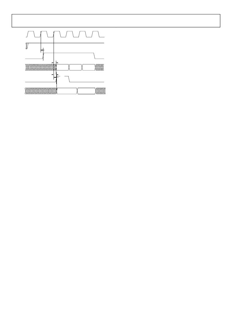
PCLKn
t
DPREQ
PxREQ
PxACK
t
DPP
Px[15:0]
I[15:0]
Q[15:0]
PxIQ
PxCH[1:0]
PxCH[0] = AGC #
PxCH[1] = 0
RSSI[11:0]
PxCH[0] = AGC #
PxCH[1] = 1
t
DPIQ
t
DPCH
0
Figure 58. AGC with RSSI Word
AVE PCLK MODES
l ports operate in either master or
via the port clock control register (Addres
l po
o
e paralle
de is set
he paralle
ntentions n the PCLK pin.
co
slave mode. The
s 0x1E).
rts power up in slave mode to avoid possible
n master m de, PCLK is an output whose frequency is the
lues for PCLK_divisor[2:1] can range from 0 to 3, integer
ors of 2, 4,or 8, respectively, can be obtained. Because the
um c
CK rate in mas
elected by setting Bit 0 of Address 0x1E.
s
hest
ode is
n slave mo e, external circuitry provides the PCLK signal.
lave-mode PCLK signals can be either synchronous or
nchrono s. The maximum slave-mode PCLK frequency is
z.
100 MH
PARALLEL PORT PIN FUNCTIONS
PCLK
Input/output. As an output (master mode), the maximum
frequency is CLK/
n
, where CLK is the AD6652 clock and
n
is a
integer divisor 1, 2, 4 or 8. As an input (slave mode), it might be
asynchronous rel
n
ative to the AD6652 CLK. This pin powers up
as an input to avoid possible contentions. Other port outputs
ange on the rising edge of PCLK.
REQ
Active high output, synchronous to PCLK. A logic high on this
s that data is available to be shifted out of the port.
gic hig
igh until all pending data has been
ted out
K
hig
ronous input. Applying a logic low on this
hibit
el port data shifting. Applying a logic high to
pin wh
is high causes the parallel port to shift out
accor
med data mode. PxACK is
pled o
lling edge of PCLK. Data is shifted out on the
ising
f PCLK after PxACK is sampled. PxACK can
eld hig
ly. In this case, when data becomes
ilable, s
s 1 PCLK cycle after the assertion of
Q (see F
igure 58).
RE
igure 55 to F
PAIQ, PBIQ
Hig
ever I data is pres
low
PAC
], PBCH[1
Th
serve to identify d
mo
e pins form a 2-b
sou
nnel of the curren
ind
he AGC source (0
indica
hether the current data word
wor
PA[
PB[15:0]
Paral
tput data por
dep
h when
.
H[1:0
ese pins
de, thes
rce cha
icates t
tes w
d (1).
15:0],
lel ou
endent.
ent on the port output, otherwise
:0]
ata in both data modes. In channel
it binary number identifying the
t data word. In AGC mode, [0]
= AGC A, 1 = AGC B), and [1]
is I/Q data (0) or a gain
ts. Contents and format are mode-
MASTER/SL
Th
mo
T
I
AD6652 clo k frequency divided by the PCLK divisor. Because
va
divis
maxim
L
P
1,
lock rate of the AD6652 is 65 MHz, the hig
ter mode is also 65 MHz. Master m
I
S
asy
ch
pin indicate
A lo
shif
PxAC
Active
pin in
this
data
sam
next r
be h
ava
h value remains h
.
h asynch
s parall
en REQ
ding to the program
n the fa
edge o
h continuous
hifting begin
相關(guān)PDF資料 |
PDF描述 |
|---|---|
| AD6652BC | 12-Bit, 65 MSPS IF to Baseband Diversity Receiver |
| AD6652PCB | 12-Bit, 65 MSPS IF to Baseband Diversity Receiver |
| AD6816 | Interface For ATM User-Network Interface IC to Category #5 Unshielded Twisted Pair (UTP) system or a fiber optic system.(ATM用戶網(wǎng)絡(luò)接口與#5類非屏蔽雙絞線系統(tǒng)或其他光纖系統(tǒng)的接口芯片) |
| AD693(中文) | Loop-Powered 4-20 mA Sensor Transmitter(環(huán)路供電,4-20mA傳感器變送器) |
| AD7010ARS | MIL-spec connector accessory |
相關(guān)代理商/技術(shù)參數(shù) |
參數(shù)描述 |
|---|---|
| AD6652BBCZ | 功能描述:IC IF TO BASEBAND RCVR 256CSPBGA RoHS:是 類別:RF/IF 和 RFID >> RF 其它 IC 和模塊 系列:- 標(biāo)準(zhǔn)包裝:100 系列:* |
| AD6652BC | 制造商:AD 制造商全稱:Analog Devices 功能描述:12-Bit, 65 MSPS IF to Baseband Diversity Receiver |
| AD6652BC/PCB | 制造商:Analog Devices 功能描述:Evaluation Board With AD6652 And Software |
| AD6652BC/PCBZ | 制造商:Analog Devices 功能描述:DUAL CHANNEL ADC WITH QUAD CHA 制造商:Analog Devices 功能描述:DUAL CHANNEL ADC WITH QUAD CHANNEL RSP - Bulk |
| AD6652PCB | 制造商:AD 制造商全稱:Analog Devices 功能描述:12-Bit, 65 MSPS IF to Baseband Diversity Receiver |
發(fā)布緊急采購,3分鐘左右您將得到回復(fù)。