- 您現(xiàn)在的位置:買賣IC網(wǎng) > PDF目錄360656 > 9S12E128DGV1 (Motorola, Inc.) MC9S12E-Family Device User Guide V01.04 PDF資料下載
參數(shù)資料
| 型號(hào): | 9S12E128DGV1 |
| 廠商: | Motorola, Inc. |
| 英文描述: | MC9S12E-Family Device User Guide V01.04 |
| 中文描述: | MC9S12E -系列設(shè)備的用戶手冊(cè)V01.04 |
| 文件頁數(shù): | 140/156頁 |
| 文件大?。?/td> | 3077K |
| 代理商: | 9S12E128DGV1 |
第1頁第2頁第3頁第4頁第5頁第6頁第7頁第8頁第9頁第10頁第11頁第12頁第13頁第14頁第15頁第16頁第17頁第18頁第19頁第20頁第21頁第22頁第23頁第24頁第25頁第26頁第27頁第28頁第29頁第30頁第31頁第32頁第33頁第34頁第35頁第36頁第37頁第38頁第39頁第40頁第41頁第42頁第43頁第44頁第45頁第46頁第47頁第48頁第49頁第50頁第51頁第52頁第53頁第54頁第55頁第56頁第57頁第58頁第59頁第60頁第61頁第62頁第63頁第64頁第65頁第66頁第67頁第68頁第69頁第70頁第71頁第72頁第73頁第74頁第75頁第76頁第77頁第78頁第79頁第80頁第81頁第82頁第83頁第84頁第85頁第86頁第87頁第88頁第89頁第90頁第91頁第92頁第93頁第94頁第95頁第96頁第97頁第98頁第99頁第100頁第101頁第102頁第103頁第104頁第105頁第106頁第107頁第108頁第109頁第110頁第111頁第112頁第113頁第114頁第115頁第116頁第117頁第118頁第119頁第120頁第121頁第122頁第123頁第124頁第125頁第126頁第127頁第128頁第129頁第130頁第131頁第132頁第133頁第134頁第135頁第136頁第137頁第138頁第139頁當(dāng)前第140頁第141頁第142頁第143頁第144頁第145頁第146頁第147頁第148頁第149頁第150頁第151頁第152頁第153頁第154頁第155頁第156頁
Device User Guide — 9S12E128DGV1/D V01.04
140
B.7.2 ATD Operating Characteristics - 3.3V Range
The
Table B-11
shows conditions under which the ATD operates.
The following constraints exist to obtain full-scale, full range results:
VSSA
≤
VRL
≤
VIN
≤
VRH
≤
VDDA
.
This constraint exists since the sample buffer amplifier can not
drive beyond the power supply levels that it ties to. If the input level goes outside of this range it will
effectively be clipped.
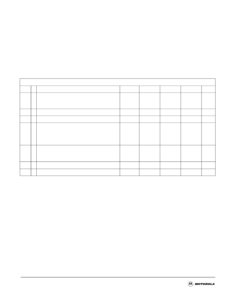
Table B-11 3.3V ATD Operating Characteristics
Conditions are shown in
Table A-4
unless otherwise noted; Supply Voltage 3.3V-10% <= V
DDA
<= 3.3V+10%
B.7.3 Factors influencing accuracy
Three factors - source resistance, source capacitance and current injection - have an influence on the
accuracy of the ATD.
B.7.3.1 Source Resistance:
Due to the input pin leakage current as specified in
Table A-6
and
Table A-7
in conjunction with the
source resistance there will be a voltage drop from the signal source to the ATD input. The maximum
source resistance R
S
specifies results in an error of less than 1/2 LSB (2.5mV) at the maximum leakage
current. If device or operating conditions are less than worst case or leakage-induced error is acceptable,
larger values of source resistance are allowed.
Num C
Rating
Symbol
Min
Typ
Max
Unit
1
D
Reference Potential
Low
High
V
RL
V
RH
V
SSA
V
DDA
/2
3.0
V
DDA
/2
V
DDA
3.6
V
V
2
C Differential Reference Voltage
V
RH
-V
RL
f
ATDCLK
3.3
V
3
D ATD Clock Frequency
0.5
2.0
MHz
4
D
ATD 10-Bit Conversion Period
Clock Cycles
1
Conv, Time at 2.0MHz ATD Clock f
ATDCLK
Conv, Time at 4.0MHz
2
ATD Clock f
ATDCLK
NOTES
:
1. The minimum time assumes a final sample period of 2 ATD clocks cycles while the maximum time assumes a final sample
period of 16 ATD clocks.
2. Reduced accuracy see
Table B-13
and
Table B-14
.
N
CONV10
T
CONV10
T
CONV10
14
7
3.5
28
14
7
Cycles
μ
s
μ
s
5
D
ATD 8-Bit Conversion Period
Clock Cycles
(1)
Conv, Time at 2.0MHz ATD Clock f
ATDCLK
N
CONV8
T
CONV8
12
6
26
13
Cycles
μ
s
6
D Recovery Time (V
DDA
=3.3 Volts)
t
REC
20
μ
s
7
P
Reference Supply current
I
REF
0.250
mA
F
For More Information On This Product,
Go to: www.freescale.com
n
.
相關(guān)PDF資料 |
PDF描述 |
|---|---|
| 9S12H128 | 16-bit Microcontroller |
| 9S12H256 | 16-bit Microcontroller |
| 9S12HN64 | 16-bit Microcontroller |
| 9S12HZ128 | 16-bit Microcontroller |
| 9S12HZ256 | 16-bit Microcontroller |
相關(guān)代理商/技術(shù)參數(shù) |
參數(shù)描述 |
|---|---|
| 9S12H128 | 制造商:FREESCALE 制造商全稱:Freescale Semiconductor, Inc 功能描述:16-bit Microcontroller |
| 9S12H256 | 制造商:FREESCALE 制造商全稱:Freescale Semiconductor, Inc 功能描述:16-bit Microcontroller |
| 9S12H256BDGV1 | 制造商:未知廠家 制造商全稱:未知廠家 功能描述:9S12H256B Device Guide |
| 9S12HN64 | 制造商:FREESCALE 制造商全稱:Freescale Semiconductor, Inc 功能描述:16-bit Microcontroller |
| 9S12HZ128 | 制造商:FREESCALE 制造商全稱:Freescale Semiconductor, Inc 功能描述:16-bit Microcontroller |
發(fā)布緊急采購,3分鐘左右您將得到回復(fù)。