- 您現(xiàn)在的位置:買賣IC網(wǎng) > PDF目錄384065 > μPD45128441 (NEC Corp.) 128M-bit Synchronous DRAM(128M 同步DRAM) PDF資料下載
參數(shù)資料
| 型號(hào): | μPD45128441 |
| 廠商: | NEC Corp. |
| 英文描述: | 128M-bit Synchronous DRAM(128M 同步DRAM) |
| 中文描述: | 128兆位同步DRAM(128M的同步DRAM)的 |
| 文件頁(yè)數(shù): | 10/84頁(yè) |
| 文件大?。?/td> | 693K |
| 代理商: | ΜPD45128441 |
第1頁(yè)第2頁(yè)第3頁(yè)第4頁(yè)第5頁(yè)第6頁(yè)第7頁(yè)第8頁(yè)第9頁(yè)當(dāng)前第10頁(yè)第11頁(yè)第12頁(yè)第13頁(yè)第14頁(yè)第15頁(yè)第16頁(yè)第17頁(yè)第18頁(yè)第19頁(yè)第20頁(yè)第21頁(yè)第22頁(yè)第23頁(yè)第24頁(yè)第25頁(yè)第26頁(yè)第27頁(yè)第28頁(yè)第29頁(yè)第30頁(yè)第31頁(yè)第32頁(yè)第33頁(yè)第34頁(yè)第35頁(yè)第36頁(yè)第37頁(yè)第38頁(yè)第39頁(yè)第40頁(yè)第41頁(yè)第42頁(yè)第43頁(yè)第44頁(yè)第45頁(yè)第46頁(yè)第47頁(yè)第48頁(yè)第49頁(yè)第50頁(yè)第51頁(yè)第52頁(yè)第53頁(yè)第54頁(yè)第55頁(yè)第56頁(yè)第57頁(yè)第58頁(yè)第59頁(yè)第60頁(yè)第61頁(yè)第62頁(yè)第63頁(yè)第64頁(yè)第65頁(yè)第66頁(yè)第67頁(yè)第68頁(yè)第69頁(yè)第70頁(yè)第71頁(yè)第72頁(yè)第73頁(yè)第74頁(yè)第75頁(yè)第76頁(yè)第77頁(yè)第78頁(yè)第79頁(yè)第80頁(yè)第81頁(yè)第82頁(yè)第83頁(yè)第84頁(yè)
Preliminary Data Sheet
10
μ
PD45128441, 45128841, 45128163
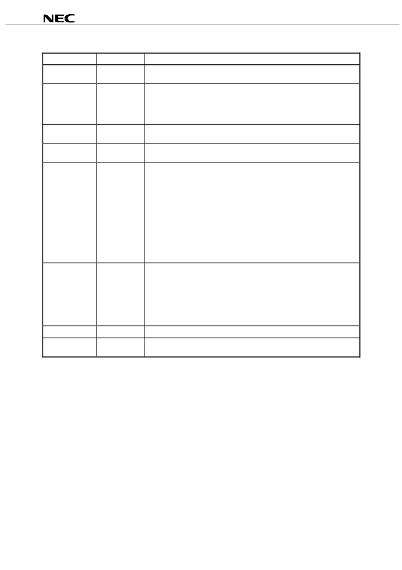
1. Input / Output Pin Function
Pin name
Input / Output
Function
CLK
Input
CLK is the master clock input. Other inputs signals are referenced to the CLK rising
edge.
CKE
Input
CKE determine validity of the next CLK (clock). If CKE is high, the next CLK rising
edge is valid; otherwise it is invalid. If the CLK rising edge is invalid, the internal clock
is not issued and the
μ
PD45128xxx suspends operation.
When the
μ
PD45128xxx is not in burst mode and CKE is negated, the device enters
power down mode. During power down mode, CKE must remain low.
/CS
Input
/CS low starts the command input cycle. When /CS is high, commands are ignored
but operations continue.
/RAS, /CAS, /WE
Input
/RAS, /CAS and /WE have the same symbols on conventional DRAM but different
functions. For details, refer to the command table.
A0 - A13
Input
Row Address is determined by A0 - A13 at the CLK (clock) rising edge in the active
command cycle. It does not depend on the bit organization.
Column Address is determined by A0 - A9, A11 at the CLK rising edge in the read or
write command cycle. It depends on the bit organization : A0 - A9, A11 for
×
4 device,
A0 - A9 for
×
8 device, A0 - A8 for
×
16 device.
A12 and A13 are the bank select signal (BS). In command cycle, A12 and A13 low
select bank A, A12 low and A13 high select bank B, A12 high and A13 low select bank
C and then A12 and A13 high select bank D.
A10 defines the precharge mode. When A10 is high in the precharge command cycle,
all banks are precharged; when A10 is low, only the bank selected by A12 and A13 is
precharged.
When A10 is high in read or write command cycle, the precharge starts automatically
after the burst access.
DQM, UDQM,
LDQM
Input
DQM controls I/O buffers. In
×
16 products, UDQM and LDQM control upper byte and
lower byte I/O buffers, respectively.
In read mode, DQM controls the output buffers like a conventional /OE pin.
DQM high and DQM low turn the output buffers off and on, respectively.
The DQM latency for the read is two clocks.
In write mode, DQM controls the word mask. Input data is written to the memory cell if
DQM is low but not if DQM is high.
The DQM latency for the write is zero.
DQ0 - DQ15
Input / Output
DQ pins have the same function as I/O pins on a conventional DRAM.
V
CC
, V
SS
, V
CC
Q,
V
SS
Q
(Power supply)
V
CC
and V
SS
are power supply pins for internal circuits. V
CC
Q and V
SS
Q are power
supply pins for the output buffers.
相關(guān)PDF資料 |
PDF描述 |
|---|---|
| μPD4516161A | 16M-bit Synchronous DRAM(16M 同步動(dòng)態(tài)RAM) |
| μPD4516421A | 16M-bit Synchronous DRAM(16M 同步動(dòng)態(tài)RAM) |
| μPD4516821A | 16M-bit Synchronous DRAM(16M 同步動(dòng)態(tài)RAM) |
| μPD45256163 | 256M-Bit Synchronous DRAM(256M 同步 動(dòng)態(tài)RAM) |
| μPD45256441 | 256M-Bit Synchronous DRAM(256M 同步 動(dòng)態(tài)RAM) |
相關(guān)代理商/技術(shù)參數(shù) |
參數(shù)描述 |
|---|---|
| PD45128441G5 | 制造商:ELPIDA 制造商全稱:Elpida Memory 功能描述:128M-bit Synchronous DRAM 4-bank, LVTTL WTR (Wide Temperature Range) |
| PD45128441G5-A10I-9JF | 制造商:ELPIDA 制造商全稱:Elpida Memory 功能描述:128M-bit Synchronous DRAM 4-bank, LVTTL WTR (Wide Temperature Range) |
| PD45128441G5-A10LI-9JF | 制造商:ELPIDA 制造商全稱:Elpida Memory 功能描述:128M-bit Synchronous DRAM 4-bank, LVTTL WTR (Wide Temperature Range) |
| PD45128441G5-A10LT-9JF | 制造商:ELPIDA 制造商全稱:Elpida Memory 功能描述:128M-bit Synchronous DRAM 4-bank, LVTTL WTR (Wide Temperature Range) |
| PD45128441G5-A10T-9JF | 制造商:ELPIDA 制造商全稱:Elpida Memory 功能描述:128M-bit Synchronous DRAM 4-bank, LVTTL WTR (Wide Temperature Range) |
發(fā)布緊急采購(gòu),3分鐘左右您將得到回復(fù)。