- 您現(xiàn)在的位置:買賣IC網(wǎng) > PDF目錄4265 > XC3S1400AN-5FGG484C (Xilinx Inc)IC FPGA SPARTAN-3AN 484FPGA PDF資料下載
參數(shù)資料
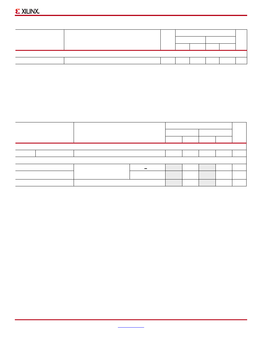
| 型號: | XC3S1400AN-5FGG484C |
| 廠商: | Xilinx Inc |
| 文件頁數(shù): | 74/123頁 |
| 文件大?。?/td> | 0K |
| 描述: | IC FPGA SPARTAN-3AN 484FPGA |
| 標準包裝: | 60 |
| 系列: | Spartan®-3AN |
| LAB/CLB數(shù): | 2816 |
| 邏輯元件/單元數(shù): | 25344 |
| RAM 位總計: | 589824 |
| 輸入/輸出數(shù): | 372 |
| 門數(shù): | 1400000 |
| 電源電壓: | 1.14 V ~ 1.26 V |
| 安裝類型: | 表面貼裝 |
| 工作溫度: | 0°C ~ 85°C |
| 封裝/外殼: | 484-BBGA |
| 供應(yīng)商設(shè)備封裝: | 484-FBGA |
第1頁第2頁第3頁第4頁第5頁第6頁第7頁第8頁第9頁第10頁第11頁第12頁第13頁第14頁第15頁第16頁第17頁第18頁第19頁第20頁第21頁第22頁第23頁第24頁第25頁第26頁第27頁第28頁第29頁第30頁第31頁第32頁第33頁第34頁第35頁第36頁第37頁第38頁第39頁第40頁第41頁第42頁第43頁第44頁第45頁第46頁第47頁第48頁第49頁第50頁第51頁第52頁第53頁第54頁第55頁第56頁第57頁第58頁第59頁第60頁第61頁第62頁第63頁第64頁第65頁第66頁第67頁第68頁第69頁第70頁第71頁第72頁第73頁當前第74頁第75頁第76頁第77頁第78頁第79頁第80頁第81頁第82頁第83頁第84頁第85頁第86頁第87頁第88頁第89頁第90頁第91頁第92頁第93頁第94頁第95頁第96頁第97頁第98頁第99頁第100頁第101頁第102頁第103頁第104頁第105頁第106頁第107頁第108頁第109頁第110頁第111頁第112頁第113頁第114頁第115頁第116頁第117頁第118頁第119頁第120頁第121頁第122頁第123頁
Spartan-3AN FPGA Family: DC and Switching Characteristics
DS557 (v4.1) April 1, 2011
Product Specification
54
Digital Frequency Synthesizer (DFS)
Delay Lines
DCM_DELAY_STEP(5)
Finest delay resolution, average over all taps
All
15
35
15
35
ps
Notes:
1.
2.
Indicates the maximum amount of output jitter that th
e DCM adds to the jitter on the CLKIN input.
3.
For optimal jitter tolerance and faster lock time, use the CLKIN_PERIOD attribute.
4.
Some jitter and duty-cycle specifications include 1% of input clock period or 0.01 UI. For example, the data sheet specifies a maximum jitter
of “±[1% of CLKIN period + 150]”. Assume the CLKIN frequency is 100 MHz. The equivalent CLKIN period is 10 ns and 1% of 10 ns is 0.1 ns
or 100 ps. According to the data sheet, the maximum jitter is ±[100 ps + 150 ps] = ±250 ps.
5.
The typical delay step size is 23 ps.
Table 41: Recommended Operating Conditions for the DFS
Symbol
Description
Speed Grade
Units
-5
-4
Min
Max
Min
Max
Input Frequency Ranges(2)
FCLKIN
CLKIN_FREQ_FX
Frequency for the CLKIN input
0.200
333(3)
0.200
MHz
Input Clock Jitter Tolerance(4)
CLKIN_CYC_JITT_FX_LF
Cycle-to-cycle jitter at the
CLKIN input, based on CLKFX
output frequency
FCLKFX < 150 MHz
–±300
ps
CLKIN_CYC_JITT_FX_HF
FCLKFX > 150 MHz
–±150
ps
CLKIN_PER_JITT_FX
Period jitter at the CLKIN input
–±1
ns
Notes:
1.
DFS specifications apply when either of the DFS outputs (CLKFX or CLKFX180) are used.
2.
If both DFS and DLL outputs are used on the same DCM, follow the more restrictive CLKIN_FREQ_DLL specifications in Table 39.
3.
To support double the maximum effective FCLKIN limit, set the CLKIN_DIVIDE_BY_2 attribute to TRUE. This attribute divides the incoming
clock frequency by two as it enters the DCM.
4.
CLKIN input jitter beyond these limits may cause the DCM to lose lock.
Table 40: Switching Characteristics for the DLL (Cont’d)
Symbol
Description
Device
Speed Grade
Units
-5
-4
Min
Max
Min
Max
相關(guān)PDF資料 |
PDF描述 |
|---|---|
| 25AA080DT-I/MNY | IC SRL EEPROM 1KX8 1.8V 8-TDFN |
| 3344-38 | SCREW BRDLOCK M2.5 0.31" 1=1PC |
| XCV50E-7PQ240C | IC FPGA 1.8V 71K GATES 240-PQFP |
| 25AA080CT-I/MNY | IC SRL EEPROM 1KX8 1.8V 8-TDFN |
| 3344-26 | SCREW BRDLOCK M2.6 0.31" 1=1PC |
相關(guān)代理商/技術(shù)參數(shù) |
參數(shù)描述 |
|---|---|
| XC3S1400AN-5FGG676C | 功能描述:IC FPGA SPARTAN -3N1400K 676FBGA RoHS:是 類別:集成電路 (IC) >> 嵌入式 - FPGA(現(xiàn)場可編程門陣列) 系列:Spartan®-3AN 標準包裝:60 系列:XP LAB/CLB數(shù):- 邏輯元件/單元數(shù):10000 RAM 位總計:221184 輸入/輸出數(shù):244 門數(shù):- 電源電壓:1.71 V ~ 3.465 V 安裝類型:表面貼裝 工作溫度:0°C ~ 85°C 封裝/外殼:388-BBGA 供應(yīng)商設(shè)備封裝:388-FPBGA(23x23) 其它名稱:220-1241 |
| XC3S1500 | 制造商:XILINX 制造商全稱:XILINX 功能描述:Spartan-3 FPGA |
| XC3S1500-4CP132C | 制造商:XILINX 制造商全稱:XILINX 功能描述:Spartan-3 FPGA |
| XC3S1500-4CP132I | 制造商:XILINX 制造商全稱:XILINX 功能描述:Spartan-3 FPGA |
| XC3S1500-4CPG132C | 制造商:XILINX 制造商全稱:XILINX 功能描述:Spartan-3 FPGA Family: Complete Data Sheet |
發(fā)布緊急采購,3分鐘左右您將得到回復。