- 您現(xiàn)在的位置:買賣IC網(wǎng) > PDF目錄359384 > VL6524 (意法半導(dǎo)體) VGA single-chip camera module PDF資料下載
參數(shù)資料
| 型號(hào): | VL6524 |
| 廠商: | 意法半導(dǎo)體 |
| 英文描述: | VGA single-chip camera module |
| 中文描述: | 顯卡單芯片相機(jī)模塊 |
| 文件頁數(shù): | 14/70頁 |
| 文件大小: | 505K |
| 代理商: | VL6524 |
第1頁第2頁第3頁第4頁第5頁第6頁第7頁第8頁第9頁第10頁第11頁第12頁第13頁當(dāng)前第14頁第15頁第16頁第17頁第18頁第19頁第20頁第21頁第22頁第23頁第24頁第25頁第26頁第27頁第28頁第29頁第30頁第31頁第32頁第33頁第34頁第35頁第36頁第37頁第38頁第39頁第40頁第41頁第42頁第43頁第44頁第45頁第46頁第47頁第48頁第49頁第50頁第51頁第52頁第53頁第54頁第55頁第56頁第57頁第58頁第59頁第60頁第61頁第62頁第63頁第64頁第65頁第66頁第67頁第68頁第69頁第70頁
Operational modes
VL6524/VS6524
14/70
During the power-up sequence (CE = logic 1)
The digital supplies must be on and stable.
The internal digital supply of the VL6524/VS6524 is enabled by an internal switch
mechanism.
All internal registers are reset to default values by an internal power on reset cell.
●
●
●
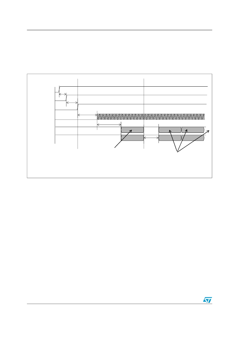
Figure 3.
Power up sequence
STANDBY mode:
The VL6524/VS6524 enters STANDBY mode when the CE pin on the
device is pulled HIGH. Power consumption is very low, most clocks inside the device are
switched off.
In this state I2C communication is possible when CLK is present and when the
microprocessor is enabled by writing the value 0x06 to the MicroEnable register 0xC003
(
Table 7
).
All registers are reset to their default values. The device I/O pins have a very high-
impedance.
Note:
On exit from STANDBY mode, the VL6524/VS6524 is in a transient mode called
UNINITIALISED, this mode is not a user mode.
STOP mode:
This is a low power mode. The analogue section of the VL6524/VS6524 is
switched off and all registers are accessed over the I2C interface. A run command received
in this state automatically sets a transition through the PAUSE state to the run mode.
PAUSE mode:
In this mode all VL6524/VS6524 clocks are running and all registers are
accessible but no data is output from the device. The device is ready to start streaming but
is halted. This mode is used to set up the required output format before outputting any data.
Note:
The PowerManagement register bTimeToPowerdown can be adjusted in PAUSE mode but
has no effect until the next RUN to PAUSE transition (
Table 13
).
RUN mode:
This is the fully operational mode.
CE
CLK
AVDD (2.8V)
VDD (1.8V/2.8V)
SDA
SCL
t1
t2
t3
t4
t1 >= 0ns
t2 >= 0ns
t3 >= 0ns
t4 >= 25ms
Constraints:
t5
low level command:enable clocks
setup commands
t5 >= 2ms
standby
POWER DOWN
相關(guān)PDF資料 |
PDF描述 |
|---|---|
| VL68C45R-35PC | Non-VGA Video Controller |
| VL68C45R-35QC | Non-VGA Video Controller |
| VL68C45S-23CC | Non-VGA Video Controller |
| VL68C45S-23PC | Non-VGA Video Controller |
| VL68C45S-23QC | Non-VGA Video Controller |
相關(guān)代理商/技術(shù)參數(shù) |
參數(shù)描述 |
|---|---|
| VL6524Q0MH | 制造商:STMicroelectronics 功能描述:VGA SINGLE-CHIP CAMERA MODULE - Trays |
| VL6524QOMH | 制造商:STMICROELECTRONICS 制造商全稱:STMicroelectronics 功能描述:VGA single-chip camera module |
| VL66 | 制造商:SPECOTECH 功能描述:Camera;IR;Weatherproof;Color;420Lines;3.7-12mmAutoIrisLens;12VDC; Black |
| VL6616 | 制造商:PRO SIGNAL 功能描述:CABLE, 4PIN MDIN PLUG, BLUE, 15M |
| VL6624 | 制造商:STMICROELECTRONICS 制造商全稱:STMicroelectronics 功能描述:1.3 Megapixel single-chip camera module |
發(fā)布緊急采購,3分鐘左右您將得到回復(fù)。