- 您現(xiàn)在的位置:買賣IC網(wǎng) > PDF目錄383983 > UPD75236GJ (NEC Corp.) DIODE ZENER SINGLE 500mW 75Vz 1.7mA-Izt 0.05 0.1uA-Ir 56Vr DO35-GLASS 5K/AMMO PDF資料下載
參數(shù)資料
| 型號: | UPD75236GJ |
| 廠商: | NEC Corp. |
| 英文描述: | DIODE ZENER SINGLE 500mW 75Vz 1.7mA-Izt 0.05 0.1uA-Ir 56Vr DO35-GLASS 5K/AMMO |
| 中文描述: | 4位單片機 |
| 文件頁數(shù): | 54/190頁 |
| 文件大小: | 1220K |
| 代理商: | UPD75236GJ |
第1頁第2頁第3頁第4頁第5頁第6頁第7頁第8頁第9頁第10頁第11頁第12頁第13頁第14頁第15頁第16頁第17頁第18頁第19頁第20頁第21頁第22頁第23頁第24頁第25頁第26頁第27頁第28頁第29頁第30頁第31頁第32頁第33頁第34頁第35頁第36頁第37頁第38頁第39頁第40頁第41頁第42頁第43頁第44頁第45頁第46頁第47頁第48頁第49頁第50頁第51頁第52頁第53頁當前第54頁第55頁第56頁第57頁第58頁第59頁第60頁第61頁第62頁第63頁第64頁第65頁第66頁第67頁第68頁第69頁第70頁第71頁第72頁第73頁第74頁第75頁第76頁第77頁第78頁第79頁第80頁第81頁第82頁第83頁第84頁第85頁第86頁第87頁第88頁第89頁第90頁第91頁第92頁第93頁第94頁第95頁第96頁第97頁第98頁第99頁第100頁第101頁第102頁第103頁第104頁第105頁第106頁第107頁第108頁第109頁第110頁第111頁第112頁第113頁第114頁第115頁第116頁第117頁第118頁第119頁第120頁第121頁第122頁第123頁第124頁第125頁第126頁第127頁第128頁第129頁第130頁第131頁第132頁第133頁第134頁第135頁第136頁第137頁第138頁第139頁第140頁第141頁第142頁第143頁第144頁第145頁第146頁第147頁第148頁第149頁第150頁第151頁第152頁第153頁第154頁第155頁第156頁第157頁第158頁第159頁第160頁第161頁第162頁第163頁第164頁第165頁第166頁第167頁第168頁第169頁第170頁第171頁第172頁第173頁第174頁第175頁第176頁第177頁第178頁第179頁第180頁第181頁第182頁第183頁第184頁第185頁第186頁第187頁第188頁第189頁第190頁
54
μ
PD75236
(4)
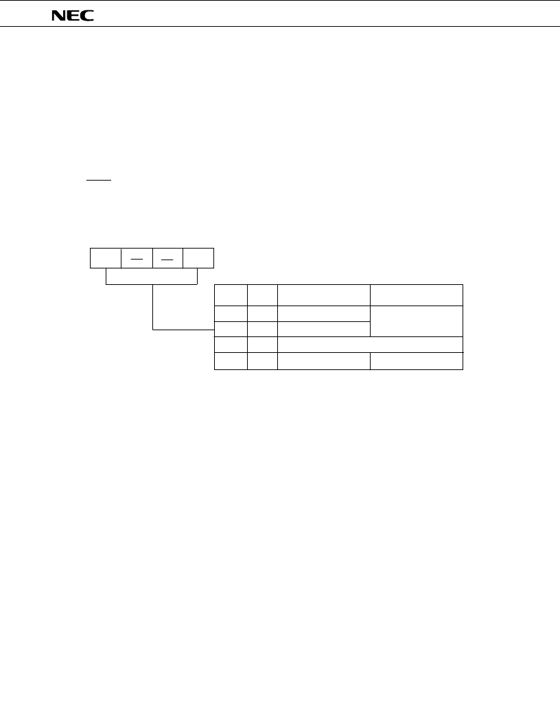
System clock control register (SCC)
The SCC is a 4-bit register to select the CPU clock
Φ
with the least significant bit and to control main
system clock oscillation stop with the most significant bit (refer to
Fig. 4-16 System Clock Control Register
Format
).
Although SCC.0 and SCC.3 are located at the same data memory address, both bits cannot be changed
simultaneously. Thus, SCC.0 and SCC.3 are set by the bit manipulation instruction. SCC.0 and SCC.3 can
always be bit manipulated irrespective of the MBE contents.
Main system clock oscillation can be stopped by setting SCC.3 only when in operation with the sub-
system clock. Oscillation when in operation with the main system clock is stopped by the STOP instruc-
tion.
RESET input clears SCC to “0”.
Fig. 4-16 System Clock Control Register Format
FB7H
SCC3
SCC0
SCC
3
2
1
0
Address
Symbol
0
0
1
1
Main system clock
Subsystem clock
Subsystem clock
Oscillation enabled
Oscillation stop
System Clock
Selection
Main System Clock
Oscillation
Setting prohibited
SCC3
SCC0
Note
1. A maximum of 1/f
XT
is required to change the system clock. Thus, when stopping the main system
clock oscillation, change the clock to the subsystem clock and set SCC.3 following the passage of
more than the machine cycles described in Table 4-2.
2. The normal STOP mode cannot be set if oscillation is stopped by setting SCC.3 while in operation
with the main system clock.
3. If SCC.3 is set to “1”, X1 input is internally short-circuited to V
SS
(GND potential) to suppress
crystal oscillator leakage. Thus, when using an external clock for the main system clock do not set
SCC.3 to “1”.
4. When PCC = 0001B (
Φ
= f
X
/16 selected), do not set SCC.0 to “1”. When switching from the main
system clock to the subsystem clock, do so after setting PCC to another value (PCC
≠
0001B).
Do not set PCC = 0001B while in operation with the subsystem clock.
0
1
0
1
相關(guān)PDF資料 |
PDF描述 |
|---|---|
| UPD75236 | 4-BIT SINGLE-CHIP MICROCOMPUTER |
| UPD75516 | 4-BIT, SINGLE-CHIP CMOS MICROCOMPUTER WITH EXTENSIVE I/O AND A/D CONVERTER |
| UPD75516GF-637-3B9 | 4-BIT SINGLE-CHIP MICROCOMPUTER |
| UPD75516GF-076 | 4-BIT SINGLE-CHIP MICROCOMPUTER |
| UPD75516GF-079 | 4-BIT SINGLE-CHIP MICROCOMPUTER |
相關(guān)代理商/技術(shù)參數(shù) |
參數(shù)描述 |
|---|---|
| UPD753012AGC-P33-8BT-A | 制造商:Renesas Electronics Corporation 功能描述: |
| UPD753016AGC-P29-8BT | 制造商:Renesas Electronics Corporation 功能描述: |
| UPD75304GF-407-3B9 | 制造商:Renesas Electronics Corporation 功能描述: |
| UPD75306G182 | 制造商:Panasonic Industrial Company 功能描述:IC |
| UPD75308F478 | 制造商:Panasonic Industrial Company 功能描述:IC |
發(fā)布緊急采購,3分鐘左右您將得到回復。