- 您現(xiàn)在的位置:買賣IC網(wǎng) > PDF目錄383983 > UPD75236GJ (NEC Corp.) DIODE ZENER SINGLE 500mW 75Vz 1.7mA-Izt 0.05 0.1uA-Ir 56Vr DO35-GLASS 5K/AMMO PDF資料下載
參數(shù)資料
| 型號: | UPD75236GJ |
| 廠商: | NEC Corp. |
| 英文描述: | DIODE ZENER SINGLE 500mW 75Vz 1.7mA-Izt 0.05 0.1uA-Ir 56Vr DO35-GLASS 5K/AMMO |
| 中文描述: | 4位單片機(jī) |
| 文件頁數(shù): | 116/190頁 |
| 文件大小: | 1220K |
| 代理商: | UPD75236GJ |
第1頁第2頁第3頁第4頁第5頁第6頁第7頁第8頁第9頁第10頁第11頁第12頁第13頁第14頁第15頁第16頁第17頁第18頁第19頁第20頁第21頁第22頁第23頁第24頁第25頁第26頁第27頁第28頁第29頁第30頁第31頁第32頁第33頁第34頁第35頁第36頁第37頁第38頁第39頁第40頁第41頁第42頁第43頁第44頁第45頁第46頁第47頁第48頁第49頁第50頁第51頁第52頁第53頁第54頁第55頁第56頁第57頁第58頁第59頁第60頁第61頁第62頁第63頁第64頁第65頁第66頁第67頁第68頁第69頁第70頁第71頁第72頁第73頁第74頁第75頁第76頁第77頁第78頁第79頁第80頁第81頁第82頁第83頁第84頁第85頁第86頁第87頁第88頁第89頁第90頁第91頁第92頁第93頁第94頁第95頁第96頁第97頁第98頁第99頁第100頁第101頁第102頁第103頁第104頁第105頁第106頁第107頁第108頁第109頁第110頁第111頁第112頁第113頁第114頁第115頁當(dāng)前第116頁第117頁第118頁第119頁第120頁第121頁第122頁第123頁第124頁第125頁第126頁第127頁第128頁第129頁第130頁第131頁第132頁第133頁第134頁第135頁第136頁第137頁第138頁第139頁第140頁第141頁第142頁第143頁第144頁第145頁第146頁第147頁第148頁第149頁第150頁第151頁第152頁第153頁第154頁第155頁第156頁第157頁第158頁第159頁第160頁第161頁第162頁第163頁第164頁第165頁第166頁第167頁第168頁第169頁第170頁第171頁第172頁第173頁第174頁第175頁第176頁第177頁第178頁第179頁第180頁第181頁第182頁第183頁第184頁第185頁第186頁第187頁第188頁第189頁第190頁
116
μ
PD75236
(4)
SA register (SA)
The SA register (Successive Approximation Register) is an 8-bit register to store the result of A/D
conversion by successive approximation.
The SA register is read by an 8-bit manipulation instruction. Data cannot be written to this register by
software.
RESET input sets the SA register to 7FH.
(5)
A/D converter operations
The analog input signal to undergo A/D conversion is specified by setting bits 6, 5 and 4 (ADM6, 5 and
4) of the A/D conversion mode register.
A/D conversion is started by setting (1) ADM bit 3 (SOC). SOC is automatically cleared (0) after the
setting. A/D conversion is executed using successive approximation by hardware and the 8-bit conversion
result data is stored into the SA register. Upon termination of conversion, bit 2 (EOC) of ADM is set (1).
Fig. 4-64 is an A/D conversion timing chart.
Use the A/D converter as follows.
Select the analog input channel (ADM 6, 5 and 4 setting).
Instruct A/D conversion start (SOC setting).
Wait for A/D conversion to terminate (wait for EOC to be set or wait with a software timer).
Read the A/D conversion result (SA register reading).
4
Note
1.
and
can be carried out simultaneously.
2. A maximum delay of 2
4
/f
X
sec (3.81
μ
s: at 4.19 MHz operation) occurs from A/D conversion start to
EOC clear after SOC setting. Thus, test EOC after the passage of time indicated in Table 4-11 after
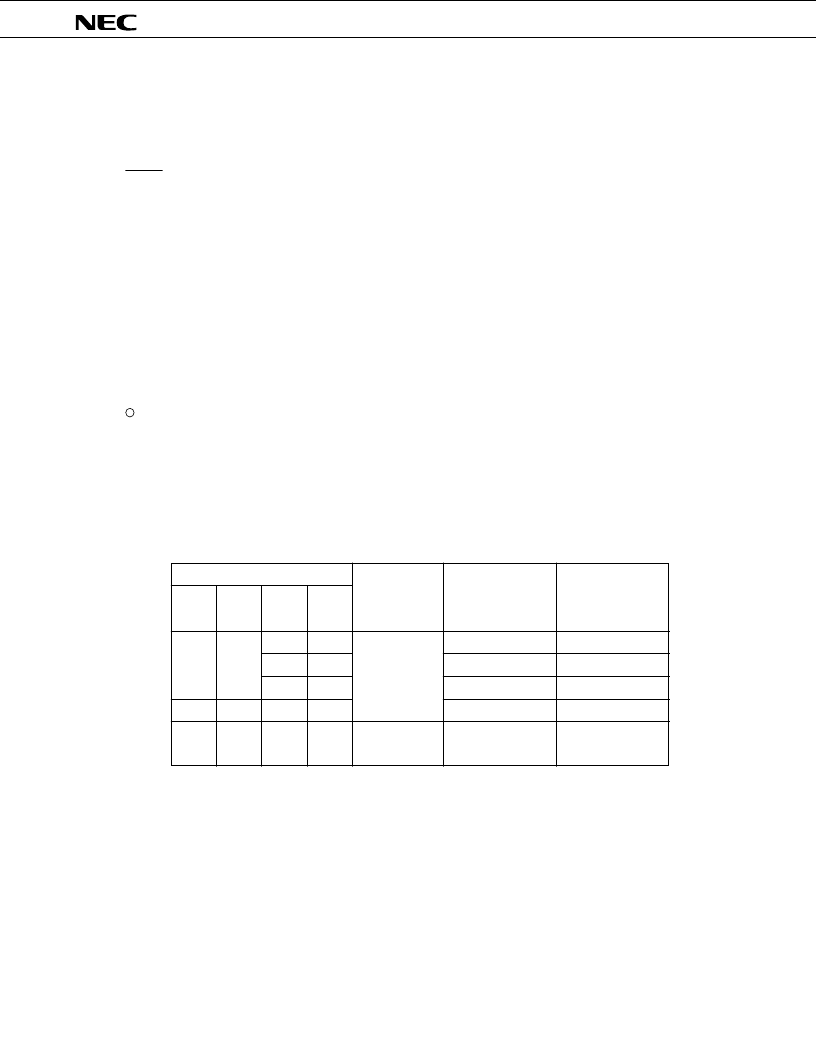
SOC setting. Table 4-7 shows A/D conversion times as well.
Table 4-7 SCC and PCC Settings
SCC and PCC Set Value
A/D Conversion
Time
Wait not required
2 machine cycles
4 machine cycles
Wait not required
Wait time till EOC
test after SOC
setting
Wait time till the
end of A/D conver-
sion after SOC
setting
3 machine cycles
21 machine cycles
42 machine cycles
Wait not required
Conversion
operation
stopped
—
—
168/f
x
(40.1
μ
s : at 4.19
MHz operation)
Remarks
x : Don’t care
SCC3
SCC0
PCC1
PCC0
0
0
0
0
1
0
1
1
0
1
×
×
1
×
×
×
相關(guān)PDF資料 |
PDF描述 |
|---|---|
| UPD75236 | 4-BIT SINGLE-CHIP MICROCOMPUTER |
| UPD75516 | 4-BIT, SINGLE-CHIP CMOS MICROCOMPUTER WITH EXTENSIVE I/O AND A/D CONVERTER |
| UPD75516GF-637-3B9 | 4-BIT SINGLE-CHIP MICROCOMPUTER |
| UPD75516GF-076 | 4-BIT SINGLE-CHIP MICROCOMPUTER |
| UPD75516GF-079 | 4-BIT SINGLE-CHIP MICROCOMPUTER |
相關(guān)代理商/技術(shù)參數(shù) |
參數(shù)描述 |
|---|---|
| UPD753012AGC-P33-8BT-A | 制造商:Renesas Electronics Corporation 功能描述: |
| UPD753016AGC-P29-8BT | 制造商:Renesas Electronics Corporation 功能描述: |
| UPD75304GF-407-3B9 | 制造商:Renesas Electronics Corporation 功能描述: |
| UPD75306G182 | 制造商:Panasonic Industrial Company 功能描述:IC |
| UPD75308F478 | 制造商:Panasonic Industrial Company 功能描述:IC |
發(fā)布緊急采購,3分鐘左右您將得到回復(fù)。