- 您現(xiàn)在的位置:買賣IC網(wǎng) > PDF目錄383982 > UPD6708GS (NEC Corp.) IEBusa Inter Equipment Busa PROTOCOL CONTROL LSI PDF資料下載
參數(shù)資料
| 型號: | UPD6708GS |
| 廠商: | NEC Corp. |
| 英文描述: | IEBusa Inter Equipment Busa PROTOCOL CONTROL LSI |
| 中文描述: | IEBusa設(shè)備布薩間協(xié)議控制大規(guī)模集成電路 |
| 文件頁數(shù): | 5/72頁 |
| 文件大小: | 292K |
| 代理商: | UPD6708GS |
第1頁第2頁第3頁第4頁當前第5頁第6頁第7頁第8頁第9頁第10頁第11頁第12頁第13頁第14頁第15頁第16頁第17頁第18頁第19頁第20頁第21頁第22頁第23頁第24頁第25頁第26頁第27頁第28頁第29頁第30頁第31頁第32頁第33頁第34頁第35頁第36頁第37頁第38頁第39頁第40頁第41頁第42頁第43頁第44頁第45頁第46頁第47頁第48頁第49頁第50頁第51頁第52頁第53頁第54頁第55頁第56頁第57頁第58頁第59頁第60頁第61頁第62頁第63頁第64頁第65頁第66頁第67頁第68頁第69頁第70頁第71頁第72頁
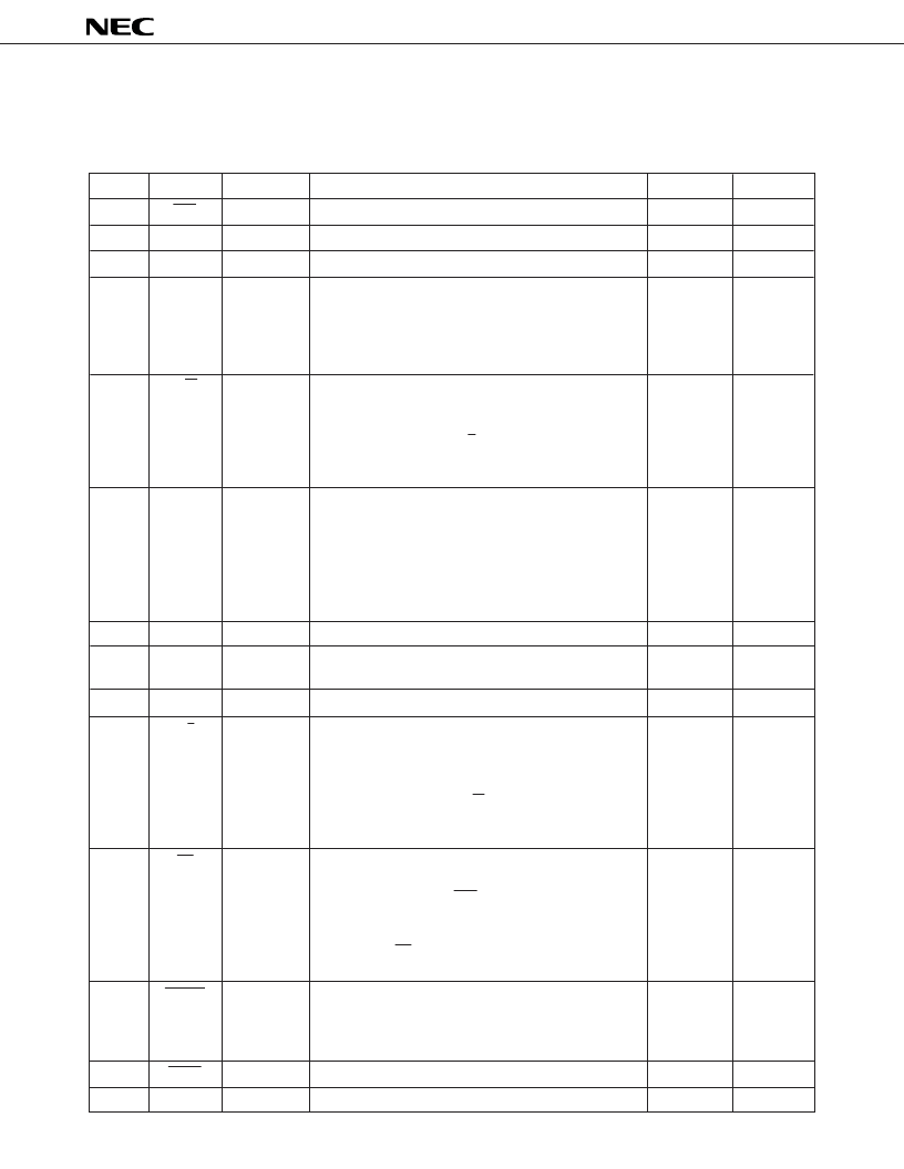
5
μ
PD6708
1.
PIN FUNCTIONS
1.1
List of Pin Functions
Pin No.
Pin Name
Input/Output
Function
I/O Format
At Reset
1
SCK
Input
Input for serial clock used to interface with microcontroller.
CMOS input
Input
2
SI
Input
Input for serial data used to interface with microcontroller.
CMOS input
Input
3
SO
Output
Output for serial data used to interface with microcontroller.
CMOS output
High level
4
IRQ
Output
Output used by interrupt request signals generated by
communication and command execution results.
Used as operation start request signal to microcontroller.
The interrupt request signal is output for 8
μ
s or longer
at high level.
CMOS output
Low level
5
R/W
Input
Input for switching serial interface read/write mode.
When high, it is in the read mode. When low, it is in the
write mode.
When this pin is low and C/D pin high, the read and write
modes can be switched by commands input from the serial
interface.
CMOS input
Input
6
7
XI
XO
––
Connection pins for system clock resonator.
Use a 12- or 12.58-MHz crystal, or ceramic resonator.
Frequency precision depends on the communication mode
used.
Mode 0
:
±
1.5 %
Mode 1
:
±
1.5 %
Mode 2
:
±
0.5 %
––
(Oscillation
continues)
8
GND
––
Ground
––
––
9
BUS–
BUS+
Input/output
Input/output for IEBus.
––
High
impedance
10
11
AV
DD
––
IEBus driver/receiver analog power supply. Connect to V
DD
.
––
––
12
C/D
Input
Input used to switch between processing data input to the
serial interface as commands or data.
When set to high, data is processed as commands; when
low, data is processed as data.
When this pin is high and R/W pin low, the read and write
modes can be switched by commands input from the serial
interface.
CMOS input
Input
13
CS
Input
Chip select input.
When low, serial interface input is enabled.
When high, serial clock (SCK) input is disabled, SO pin
becomes high impedance, and the serial clock counter is
reset.
The status of CS pin is not affected by IEBus transmit and
receive operations.
CMOS input
Input
14
RESET
Input
System reset signal input pin.
Low input effects a reset.
Always input the low signal for 6
μ
s or longer after turning
on the power.
CMOS input
Input
15
TEST
Input
Always connect this pin to the V
DD
.
CMOS input
––
16
V
DD
––
Positive power supply input. Apply a voltage of 5 V
±
10 %.
––
––
相關(guān)PDF資料 |
PDF描述 |
|---|---|
| UPD6951 | 6 BIT D/A CONVERTER FOR VIDEO SIGNAL PROCESSING CMOS LSI |
| UPD6951C | 6 BIT D/A CONVERTER FOR VIDEO SIGNAL PROCESSING CMOS LSI |
| UPD6951G | 6 BIT D/A CONVERTER FOR VIDEO SIGNAL PROCESSING CMOS LSI |
| UPD703130GC-8EU | MOS INTEGRATED CIRCUIT |
| UPD703130 | MOS INTEGRATED CIRCUIT |
相關(guān)代理商/技術(shù)參數(shù) |
參數(shù)描述 |
|---|---|
| UPD6708GS(A) | 制造商:Renesas Electronics Corporation 功能描述: |
| UPD67100 | 制造商:未知廠家 制造商全稱:未知廠家 功能描述:ASIC |
| UPD67101 | 制造商:未知廠家 制造商全稱:未知廠家 功能描述:ASIC |
| UPD67240 | 制造商:未知廠家 制造商全稱:未知廠家 功能描述:ASIC |
| UPD67A | 制造商:未知廠家 制造商全稱:未知廠家 功能描述:Microcontrollers for Remote Controllers Pamphlet | Pamphlet[11/2002] |
發(fā)布緊急采購,3分鐘左右您將得到回復(fù)。