- 您現(xiàn)在的位置:買賣IC網(wǎng) > PDF目錄383982 > UPD6708GS (NEC Corp.) IEBusa Inter Equipment Busa PROTOCOL CONTROL LSI PDF資料下載
參數(shù)資料
| 型號: | UPD6708GS |
| 廠商: | NEC Corp. |
| 英文描述: | IEBusa Inter Equipment Busa PROTOCOL CONTROL LSI |
| 中文描述: | IEBusa設(shè)備布薩間協(xié)議控制大規(guī)模集成電路 |
| 文件頁數(shù): | 23/72頁 |
| 文件大?。?/td> | 292K |
| 代理商: | UPD6708GS |
第1頁第2頁第3頁第4頁第5頁第6頁第7頁第8頁第9頁第10頁第11頁第12頁第13頁第14頁第15頁第16頁第17頁第18頁第19頁第20頁第21頁第22頁當前第23頁第24頁第25頁第26頁第27頁第28頁第29頁第30頁第31頁第32頁第33頁第34頁第35頁第36頁第37頁第38頁第39頁第40頁第41頁第42頁第43頁第44頁第45頁第46頁第47頁第48頁第49頁第50頁第51頁第52頁第53頁第54頁第55頁第56頁第57頁第58頁第59頁第60頁第61頁第62頁第63頁第64頁第65頁第66頁第67頁第68頁第69頁第70頁第71頁第72頁
23
μ
PD6708
4.1.4
Status register (STR)
STR is an 8-bit register used to determine the status of the
μ
PD6708.
The statuses of WDB and RDB and the status of interrupts can be read from higher 4 bits. The return code, which indicates
the result of the communication, can be read from lower 4 bits.
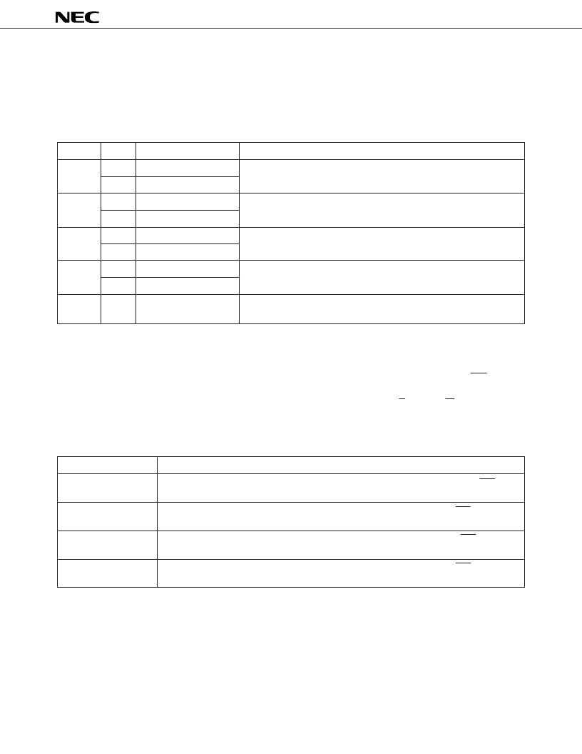
Table 4-2. Contents of Status Register
Bit
Value
Meaning
Description
Bit 7
1
WDB is full
Indicates whether data can be written to WDB
0
WDB is not full
Bit 6
1
RDB is empty
Indicates whether data can be read from RDB
0
RDB is not empty
Bit 5
1
WDB is empty
Indicates whether data is in WDB
0
WDB is not empty
Bit 4
1
Interrupt requested
Indicates whether interrupt servicing is being requested (Bit 4 of the status
register is reset by STR by the host controller)
0
Interrupt not requested
Bit 3 to
Bit 0
Return code
Return code will be read
4.2
Host Interface Modes
The host controller can access WDB, RDB, CMR, and STR within the
μ
PD6708 via the serial interface (SCK, SI, SO).
There are four modes for accessing the serial interface, as shown in the Table 4-3.
There are two method for switching among these four host interface modes: by using C/D pin and R/W pin, and by writing
data to CMR (software control).
Table 4-3. Host Interface Mode
Mode
Operation
Data write mode
Data input to SI pin is written to WDB from MSB at the rising edge of the serial clock input to SCK pin.
Data setting is completed at the eighth serial clock cycle.
Data read mode
RDB data is output from MSB to SO pin at the falling edge of the serial clock input to SCK pin. A data
read is completed by inputting eight serial clock cycles. Data at SI pin is ignored.
Command write mode
Data input to SI pin is written to CMR from MSB at rising edge of the serial clock input to SCK pin. Data
setting is completed at the eight serial clock cycle.
Status read mode
STR data is output from MSB to SO pin at the falling edge of the serial clock input to SCK pin. A data
read is completed by inputting eight serial clock cycles. Data at SI pin is ignored.
相關(guān)PDF資料 |
PDF描述 |
|---|---|
| UPD6951 | 6 BIT D/A CONVERTER FOR VIDEO SIGNAL PROCESSING CMOS LSI |
| UPD6951C | 6 BIT D/A CONVERTER FOR VIDEO SIGNAL PROCESSING CMOS LSI |
| UPD6951G | 6 BIT D/A CONVERTER FOR VIDEO SIGNAL PROCESSING CMOS LSI |
| UPD703130GC-8EU | MOS INTEGRATED CIRCUIT |
| UPD703130 | MOS INTEGRATED CIRCUIT |
相關(guān)代理商/技術(shù)參數(shù) |
參數(shù)描述 |
|---|---|
| UPD6708GS(A) | 制造商:Renesas Electronics Corporation 功能描述: |
| UPD67100 | 制造商:未知廠家 制造商全稱:未知廠家 功能描述:ASIC |
| UPD67101 | 制造商:未知廠家 制造商全稱:未知廠家 功能描述:ASIC |
| UPD67240 | 制造商:未知廠家 制造商全稱:未知廠家 功能描述:ASIC |
| UPD67A | 制造商:未知廠家 制造商全稱:未知廠家 功能描述:Microcontrollers for Remote Controllers Pamphlet | Pamphlet[11/2002] |
發(fā)布緊急采購,3分鐘左右您將得到回復(fù)。