- 您現(xiàn)在的位置:買賣IC網(wǎng) > PDF目錄384010 > TLV320AIC10I (Texas Instruments, Inc.) General-Purpose 3V to 5.5V 16-bit 22-KSPS DSP CODEC PDF資料下載
參數(shù)資料
| 型號(hào): | TLV320AIC10I |
| 廠商: | Texas Instruments, Inc. |
| 元件分類: | Codec |
| 英文描述: | General-Purpose 3V to 5.5V 16-bit 22-KSPS DSP CODEC |
| 中文描述: | 通用3V至5.5V 16位22 kSPS的DSP的解碼器 |
| 文件頁數(shù): | 11/57頁 |
| 文件大?。?/td> | 284K |
| 代理商: | TLV320AIC10I |
第1頁第2頁第3頁第4頁第5頁第6頁第7頁第8頁第9頁第10頁當(dāng)前第11頁第12頁第13頁第14頁第15頁第16頁第17頁第18頁第19頁第20頁第21頁第22頁第23頁第24頁第25頁第26頁第27頁第28頁第29頁第30頁第31頁第32頁第33頁第34頁第35頁第36頁第37頁第38頁第39頁第40頁第41頁第42頁第43頁第44頁第45頁第46頁第47頁第48頁第49頁第50頁第51頁第52頁第53頁第54頁第55頁第56頁第57頁
1–5
1.5
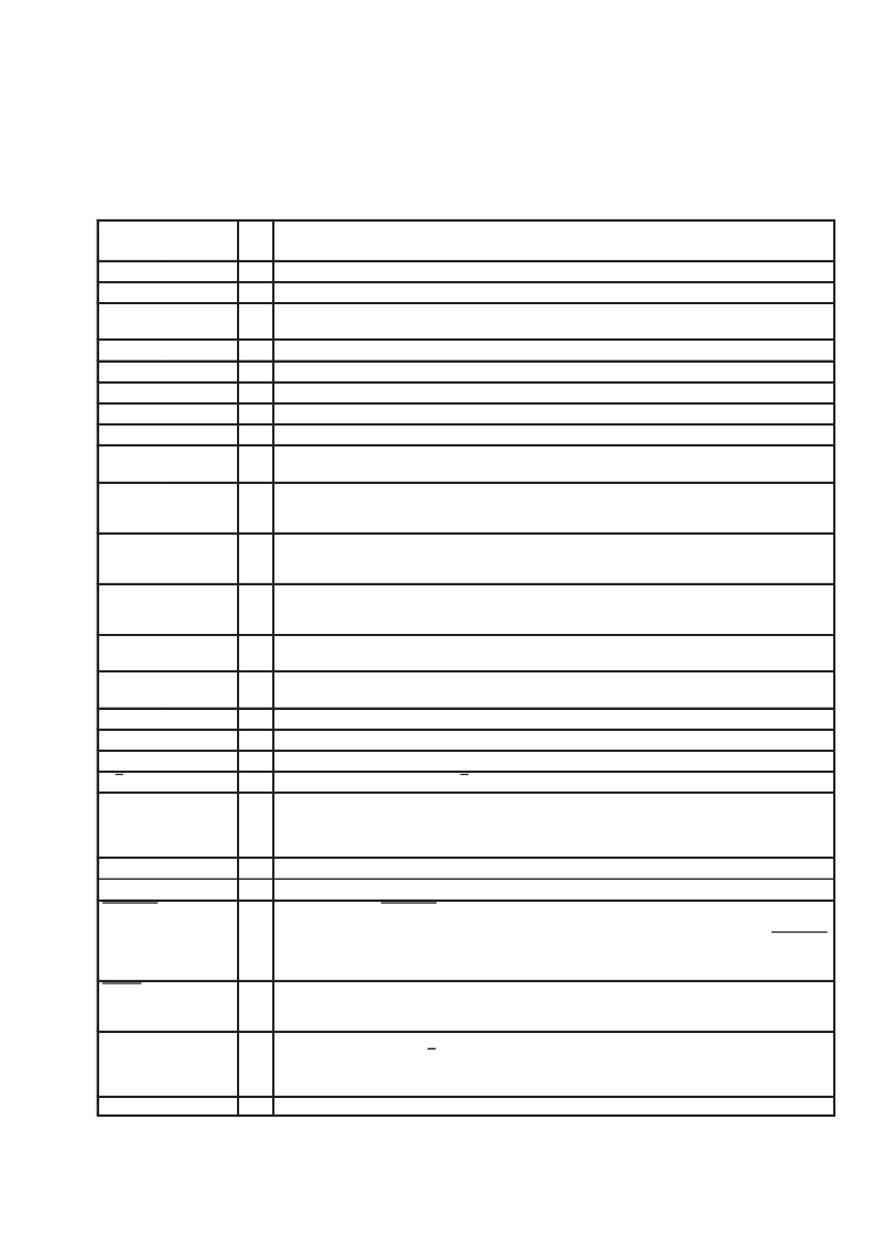
Terminal Functions (Continued)
TERMINAL
I/O
DESCRIPTION
NAME
NO.
DTXIM
7
I
Transmitter-path amplifier A3 analog inverting input. Can also be used for general-purpose amplification.
DTXIP
6
I
Transmitter-path amplifier A4 analog noninverting input. Can also be used for general-purpose amplification.
DTXOM
5
O
Transmitter path amplifier A4 feedback for negative output. Can also be used for general-purpose
amplification.
DTXOP
4
O
Transmitter path amplifier A3 feedback for positive output. Can also be used for negative output.
DVDD1
DVDD2
DVSS
FC
15
I
Digital power supply
30
I
Digital power supply
14, 29
I
Digital ground
24
I
Hardware request for secondary communication
FILT
38
O
Bandgap filter. FILT is provided for decoupling of the bandgap reference, and provides 2.5 V. The optimal
capacitor value is 0.1
μ
F (ceramic). This voltage node should be loaded only with a high-impedance dc load.
FLAG
23
O
Controlled by bit D4 of control register 3. If D4=0 (default), the FLAG pin outputs the communication flag that
goes low/high to indicate primary-communication/secondary-communication interval, respectively. If D4=1,
the FLAG pin outputs the value of D3.
FS
22
I/O
Frame sync. When FS goes low, DIN begins receiving data bits and DOUT begins transmitting data bits. In
master mode, FS is internally generated and is low during data transmission to DIN and from DOUT. In slave
mode, FS is externally generated.
FSD
21
O
Frame-sync delayed output. The FSD output synchronizes a slave device to the frame sync of the master
device. FSD is applied to the slave FS input and has the same duration as the master FS signal. Requires a
pullup resistor if not used.
INM
48
I
Inverting input to analog modulator. INM requires an external R-C antialias filter with low output impedance if
the internal antialias filter is bypassed.
INP
47
I
Noninverting input to analog modulator. INP requires an external R-C antialias filter with low output impedance
if the internal antialias filter is bypassed.
M0
10
I
Combine with M1 to select serial interface mode (frame-sync mode)
M1
11
I
Combine with M0 to select serial interface mode (frame-sync mode)
MCLK
20
I
Master clock. MCLK derives the internal clocks of the sigma-delta analog interface circuit.
M/S
27
I
Master/slave select input. When M/S is high, the device is the master, and when is low, it is a slave.
NC
18, 28, 31,
32, 35, 36,
37, 39, 41,
44
No connection
OUTM
9
O
DAC’s inverting output. OUTM is functionally identical with and complementary to OUTP.
OUTP
8
O
DAC’s noninverting output. OUTP can also be used alone for single-ended operation.
PWRDWN
12
I
Power down. When PWRDWN is pulled low, the device goes into a power-down mode, the serial interface is
disabled, and most of the high-speed clocks are disabled. However, all register values are sustained and the
device resumes full-power operation without reinitialization when PWRDWN is pulled high again. PWRDWN
resets the counters only and preserves the programmed register contents. See paragraph 2.2.2 for more
information.
RESET
13
I
Reset. The reset function is provided to initialize all the internal registers to their default values. The serial port
can be configured to the default state accordingly. See Appendix A, Register Set and Subsection 2.2.1, Reset
and Power-Down Functionsfor detailed descriptions.
SCLK
19
I/O
Shift clock. SCLK signal clocks serial data into DIN and out of DOUT during the frame-sync interval. When
configured as an output (M/S high), SCLK is generated internally by multiplying the frame-sync signal
frequency by 256 (cascade devices < 5) or 512 (cascade devices > 4). When configured as an input (M/S low),
SCLK is generated externally and must be synchronous with the master clock and frame sync.
VMID
43
O
Reference voltage output at AVDD/2
相關(guān)PDF資料 |
PDF描述 |
|---|---|
| TLV320AIC11C | General-Purpose Low-Voltage 1.1V to 3.6V/0 16-bit 22-KSPS DSP CODEC |
| TLV320AIC11I | General-Purpose Low-Voltage 1.1V to 3.6V/0 16-bit 22-KSPS DSP CODEC |
| TLV320AIC34_1 | FOUR-CHANNEL, LOW-POWER AUDIO CODEC FOR PORTABLE AUDIO/TELEPHONY |
| TLV3701CDBV | FAMILY OF NANOPOWER PUSH-PULL OUTPUT COMPARATORS |
| TLV3701IDBV | FAMILY OF NANOPOWER PUSH-PULL OUTPUT COMPARATORS |
相關(guān)代理商/技術(shù)參數(shù) |
參數(shù)描述 |
|---|---|
| TLV320AIC10IGQER | 功能描述:接口—CODEC 16-Bit 22-KSPS DSP Codec RoHS:否 制造商:Texas Instruments 類型: 分辨率: 轉(zhuǎn)換速率:48 kSPs 接口類型:I2C ADC 數(shù)量:2 DAC 數(shù)量:4 工作電源電壓:1.8 V, 2.1 V, 2.3 V to 5.5 V 最大工作溫度:+ 85 C 安裝風(fēng)格:SMD/SMT 封裝 / 箱體:DSBGA-81 封裝:Reel |
| TLV320AIC10IPFB | 功能描述:接口—CODEC 16-Bit 22-KSPS DSP Codec RoHS:否 制造商:Texas Instruments 類型: 分辨率: 轉(zhuǎn)換速率:48 kSPs 接口類型:I2C ADC 數(shù)量:2 DAC 數(shù)量:4 工作電源電壓:1.8 V, 2.1 V, 2.3 V to 5.5 V 最大工作溫度:+ 85 C 安裝風(fēng)格:SMD/SMT 封裝 / 箱體:DSBGA-81 封裝:Reel |
| TLV320AIC10IPFBG4 | 功能描述:接口—CODEC 18-Bit Regstr Bus Trncvr W/3-St Otpt RoHS:否 制造商:Texas Instruments 類型: 分辨率: 轉(zhuǎn)換速率:48 kSPs 接口類型:I2C ADC 數(shù)量:2 DAC 數(shù)量:4 工作電源電壓:1.8 V, 2.1 V, 2.3 V to 5.5 V 最大工作溫度:+ 85 C 安裝風(fēng)格:SMD/SMT 封裝 / 箱體:DSBGA-81 封裝:Reel |
| TLV320AIC10PFB | 制造商:TI 制造商全稱:Texas Instruments 功能描述:General-Purpose 3V to 5.5V 16-bit 22-KSPS DSP CODEC |
| TLV320AIC11 | 制造商:TI 制造商全稱:Texas Instruments 功能描述:General-Purpose Low-Voltage 1.1V to 3.6V/0 16-bit 22-KSPS DSP CODEC |
發(fā)布緊急采購,3分鐘左右您將得到回復(fù)。