- 您現(xiàn)在的位置:買賣IC網(wǎng) > PDF目錄383997 > THS4215DGNRG4 (Texas Instruments, Inc.) LOW-DISTORTION HIGH-SPEED VOLTAGE FEEDBACK AMPLIFIER PDF資料下載
參數(shù)資料
| 型號: | THS4215DGNRG4 |
| 廠商: | Texas Instruments, Inc. |
| 英文描述: | LOW-DISTORTION HIGH-SPEED VOLTAGE FEEDBACK AMPLIFIER |
| 中文描述: | 低失真高速電壓反饋型放大器 |
| 文件頁數(shù): | 20/41頁 |
| 文件大?。?/td> | 1591K |
| 代理商: | THS4215DGNRG4 |
第1頁第2頁第3頁第4頁第5頁第6頁第7頁第8頁第9頁第10頁第11頁第12頁第13頁第14頁第15頁第16頁第17頁第18頁第19頁當(dāng)前第20頁第21頁第22頁第23頁第24頁第25頁第26頁第27頁第28頁第29頁第30頁第31頁第32頁第33頁第34頁第35頁第36頁第37頁第38頁第39頁第40頁第41頁
www.ti.com
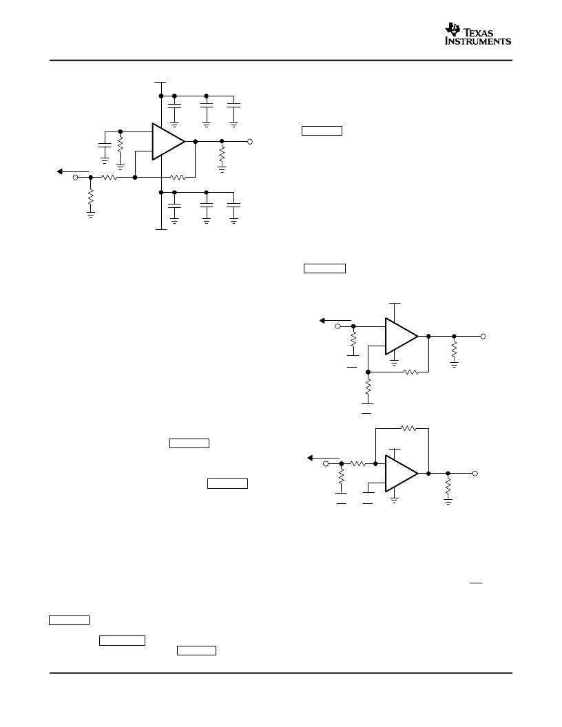
SINGLE SUPPLY OPERATION
The THS4211 is designed to operate from a single
5-V to 15-V power supply. When operating from a
single power supply, care must be taken to ensure
the input signal and amplifier are biased appropriately
to maximize output voltage swing. The circuits shown
in Figure 77 demonstrate methods to configure an
amplifier for single-supply operation.
+
THS4211
R
g
392
R
M
57.6
R
T
200
100 pF
0.1
μ
F
6.8
μ
F
-V
S
-5 V
50
Source
+
V
I
100 pF
0.1
μ
F
6.8
μ
F
+
+V
S
5 V
V
O
C
T
0.1
μ
F
R
f
392
499
_
+
THS4211
49.9
50
Source
V
I
+V
S
V
O
R
f
392
R
g
392
+V
S
2
+V
S
2
_
+
THS4211
392
R
T
50
Source
V
I
V
S
V
O
R
f
392
+V
S
2
57.6
R
g
499
R
T
499
+V
S
2
Saving Power With Power-Down
Functionality and Setting Threshold Levels
With the Reference Pin
The THS4215 features a power-down pin (PD) which
lowers the quiescent current from 19-mA down to
650-μA, ideal for reducing system power.
THS4211
THS4215
SLOS400D–SEPTEMBER 2002–REVISED NOVEMBER 2004
The last major consideration in inverting amplifier
design is setting the bias-current cancellation resistor
on the noninverting input. If the resistance is set
equal to the total dc resistance looking out of the
inverting terminal, the output dc error, due to the input
bias currents, is reduced to (input offset current)
×
R
f
in Figure 76, the dc source impedance looking out of
the inverting terminal is 392
|| (392
+ 26.8
) =
200
. To reduce the additional high-frequency noise
introduced by the resistor at the noninverting input,
and power-supply feedback, R
T
is bypassed with a
capacitor to ground.
Figure 76. Wideband, Inverting Gain
Configuration
In the inverting configuration, some key design con-
siderations must be noted. One is that the gain
resistor (R
g
) becomes part of the signal-channel input
impedance. If input impedance matching is desired
(beneficial when the signal is coupled through a
cable, twisted pair, long PC board trace, or other
transmission line conductor), R
may be set equal to
the required termination value and R
f
adjusted to give
the desired gain. However, care must be taken when
dealing with low inverting gains, as the resultant
feedback resistor value can present a significant load
to the amplifier output. For an inverting gain of 2,
setting R
to 49.9
for input matching eliminates the
need for R
M
but requires a 100-
feedback resistor.
This has the advantage that the noise gain becomes
equal to 2 for a 50-
source impedance—the same
as the noninverting circuit in Figure 75. However, the
amplifier output now sees the 100-
feedback re-
sistor in parallel with the external load. To eliminate
this excessive loading, it is preferable to increase
both R
g
and R
f
, values, as shown in Figure 76, and
then achieve the input matching impedance with a
third resistor (R
M
) to ground. The total input im-
pedance becomes the parallel combination of R
g
and
R
M
.
The next major consideration is that the signal source
impedance becomes part of the noise gain equation
and hence influences the bandwidth. For example,
the R
M
value combines in parallel with the external
50-
source impedance (at high frequencies), yield-
ing an effective source impedance of 50
|| 57.6
=
26.8
. This impedance is then added in series with
R
g
for calculating the noise gain. The result is 1.9 for
Figure 76, as opposed to the 1.8 if R
is eliminated.
The bandwidth is lower for the inverting gain-of-2
circuit
in
Figure
76
(NG=+1.9),
noninverting gain of 2 circuit in Figure 75.
Figure 77. DC-Coupled Single Supply Operation
The power-down pin of the amplifiers defaults to the
positive supply voltage in the absence of an applied
voltage, putting the amplifier in the power-on mode of
operation. To conserve power, the amplifier is turned
off by driving the power-down pin towards the nega-
than
for
the
20
相關(guān)PDF資料 |
PDF描述 |
|---|---|
| THS4215DRB | LOW-DISTORTION HIGH-SPEED VOLTAGE FEEDBACK AMPLIFIER |
| THS5651ADW | 10-BIT, 125 MSPS, CommsDACE DIGITAL-TO-ANALOG CONVERTER |
| THS5651DW | 10-BIT, 100 MSPS, CommsDACE DIGITAL-TO-ANALOG CONVERTER |
| THS5651PW | 10-BIT, 100 MSPS, CommsDACE DIGITAL-TO-ANALOG CONVERTER |
| THS5661DW | 12-BIT, 100 MSPS, CommsDACE DIGITAL-TO-ANALOG CONVERTER |
相關(guān)代理商/技術(shù)參數(shù) |
參數(shù)描述 |
|---|---|
| THS4215DR | 功能描述:高速運算放大器 Super-Fast Ultr-Lo- Distortion Hi-Speed RoHS:否 制造商:Texas Instruments 通道數(shù)量:1 電壓增益 dB:116 dB 輸入補償電壓:0.5 mV 轉(zhuǎn)換速度:55 V/us 工作電源電壓:36 V 電源電流:7.5 mA 最大工作溫度:+ 85 C 安裝風(fēng)格:SMD/SMT 封裝 / 箱體:SOIC-8 封裝:Tube |
| THS4215DRB | 制造商:Rochester Electronics LLC 功能描述:- Bulk |
| THS4215DRBR | 功能描述:高速運算放大器 Super-Fast Ultr-Lo- Distortion Hi-Speed RoHS:否 制造商:Texas Instruments 通道數(shù)量:1 電壓增益 dB:116 dB 輸入補償電壓:0.5 mV 轉(zhuǎn)換速度:55 V/us 工作電源電壓:36 V 電源電流:7.5 mA 最大工作溫度:+ 85 C 安裝風(fēng)格:SMD/SMT 封裝 / 箱體:SOIC-8 封裝:Tube |
| THS4215DRBRG4 | 功能描述:高速運算放大器 Super-Fast Ultr-Lo- Distortion Hi-Speed RoHS:否 制造商:Texas Instruments 通道數(shù)量:1 電壓增益 dB:116 dB 輸入補償電壓:0.5 mV 轉(zhuǎn)換速度:55 V/us 工作電源電壓:36 V 電源電流:7.5 mA 最大工作溫度:+ 85 C 安裝風(fēng)格:SMD/SMT 封裝 / 箱體:SOIC-8 封裝:Tube |
| THS4215DRBT | 功能描述:高速運算放大器 Super-Fast Ultr-Lo- Distortion Hi-Speed RoHS:否 制造商:Texas Instruments 通道數(shù)量:1 電壓增益 dB:116 dB 輸入補償電壓:0.5 mV 轉(zhuǎn)換速度:55 V/us 工作電源電壓:36 V 電源電流:7.5 mA 最大工作溫度:+ 85 C 安裝風(fēng)格:SMD/SMT 封裝 / 箱體:SOIC-8 封裝:Tube |
發(fā)布緊急采購,3分鐘左右您將得到回復(fù)。