- 您現(xiàn)在的位置:買賣IC網(wǎng) > PDF目錄383997 > THS4215DGNRG4 (Texas Instruments, Inc.) LOW-DISTORTION HIGH-SPEED VOLTAGE FEEDBACK AMPLIFIER PDF資料下載
參數(shù)資料
| 型號: | THS4215DGNRG4 |
| 廠商: | Texas Instruments, Inc. |
| 英文描述: | LOW-DISTORTION HIGH-SPEED VOLTAGE FEEDBACK AMPLIFIER |
| 中文描述: | 低失真高速電壓反饋型放大器 |
| 文件頁數(shù): | 19/41頁 |
| 文件大小: | 1591K |
| 代理商: | THS4215DGNRG4 |
第1頁第2頁第3頁第4頁第5頁第6頁第7頁第8頁第9頁第10頁第11頁第12頁第13頁第14頁第15頁第16頁第17頁第18頁當(dāng)前第19頁第20頁第21頁第22頁第23頁第24頁第25頁第26頁第27頁第28頁第29頁第30頁第31頁第32頁第33頁第34頁第35頁第36頁第37頁第38頁第39頁第40頁第41頁
www.ti.com
APPLICATION INFORMATION
HIGH-SPEED OPERATIONAL AMPLIFIERS
The THS4211 and the THS4215 operational ampli-
fiers set new performance levels, combining low
distortion, high slew rates, low noise, and a unity-gain
bandwidth in excess of 1 GHz. To achieve the full
performance of the amplifier, careful attention must
be paid to printed-circuit board layout and component
selection.
Applications Section Contents
Wideband, Noninverting Operation
Wideband, Inverting Gain Operation
Single Supply Operation
Saving Power With Power-Down Functionality
and Setting Threshold Levels With the Reference
Pin
Power
Supply
Decoupling
Recommendations
Using the THS4211 as a DAC Output Buffer
Driving an ADC With the THS4211
Active Filtering With the THS4211
Building a Low-Noise Receiver With the THS4211
Linearity:
Definitions,
Techniques and Design Tradeoffs
An Abbreviated Analysis of Noise in Amplifiers
Driving Capacitive Loads
Printed-Circuit
Board
Optimal Performance
Power Dissipation and Thermal Considerations
Performance vs Package Options
Evaluation
Fixtures,
Applications Support
Additional Reference Material
Mechanical Package Drawings
+
THS4211
R
f
392
49.9
100 pF
0.1
μ
F
6.8
μ
F
+
-V
S
-5 V
R
g
50
Source
V
I
100 pF
0.1
μ
F
6.8
μ
F
+
+V
S
5 V
V
O
499
392
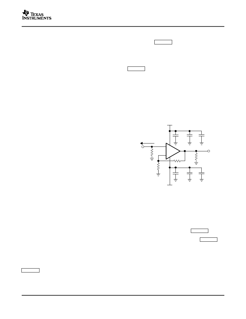
WIDEBAND, INVERTING GAIN OPERATION
Since
the
THS4211
eral-purpose, wideband voltage-feedback amplifiers,
several familiar operational-amplifier applications cir-
cuits are available to the designer. Figure 76 shows a
typical inverting configuration where the input and
output impedances and noise gain from Figure 75 are
retained in an inverting circuit configuration. Inverting
operation is a common requirement and offers sev-
eral performance benefits. The inverting configuration
shows improved slew rates and distortion due to the
pseudo-static voltage maintained on the inverting
input.
WIDEBAND, NONINVERTING OPERATION
The THS4211 and the THS4215 are unity-gain,
stable 1-GHz voltage-feedback operational amplifiers,
with and without power-down capability, designed to
operate from a single 5-V to 15-V power supply.
THS4211
THS4215
SLOS400D–SEPTEMBER 2002–REVISED NOVEMBER 2004
with measurement equipment presenting a 50-
load
impedance. In Figure 75, the 49.9-
shunt resistor at
the V
IN
terminal matches the source impedance of the
test generator. The total 499-
load at the output,
combined with the 784-
total feedback-network
load, presents the THS4211 and THS4215 with an
effective output load of 305
for the circuit shown in
Figure 75.
Voltage-feedback amplifiers, unlike current-feedback
designs, can use a wide range of resistors values to
set their gain with minimal impact on their stability
and frequency response. Larger-valued resistors de-
crease the loading effect of the feedback network on
the output of the amplifier, but this enhancement
comes at the expense of additional noise and poten-
tially lower bandwidth. Feedback-resistor values be-
tween 392
and 1 k
are recommended for most
applications.
The THS4215 provides a power-down mode, provid-
ing the ability to save power when the amplifier is
inactive. A reference pin is provided to allow the user
the flexibility to control the threshold levels of the
power-down control pin.
Techniques
and
Terminology,
Circuit
Figure 75. Wideband, Noninverting Gain
Configuration
Layout
Techniques
for
and
THS4215
are
gen-
Spice
Models,
and
Figure 75 shows the noninverting-gain configuration
of 2 V/V used to demonstrate the typical performance
curves. Most of the curves were characterized using
signal sources with 50-
source impedances, and
19
相關(guān)PDF資料 |
PDF描述 |
|---|---|
| THS4215DRB | LOW-DISTORTION HIGH-SPEED VOLTAGE FEEDBACK AMPLIFIER |
| THS5651ADW | 10-BIT, 125 MSPS, CommsDACE DIGITAL-TO-ANALOG CONVERTER |
| THS5651DW | 10-BIT, 100 MSPS, CommsDACE DIGITAL-TO-ANALOG CONVERTER |
| THS5651PW | 10-BIT, 100 MSPS, CommsDACE DIGITAL-TO-ANALOG CONVERTER |
| THS5661DW | 12-BIT, 100 MSPS, CommsDACE DIGITAL-TO-ANALOG CONVERTER |
相關(guān)代理商/技術(shù)參數(shù) |
參數(shù)描述 |
|---|---|
| THS4215DR | 功能描述:高速運(yùn)算放大器 Super-Fast Ultr-Lo- Distortion Hi-Speed RoHS:否 制造商:Texas Instruments 通道數(shù)量:1 電壓增益 dB:116 dB 輸入補(bǔ)償電壓:0.5 mV 轉(zhuǎn)換速度:55 V/us 工作電源電壓:36 V 電源電流:7.5 mA 最大工作溫度:+ 85 C 安裝風(fēng)格:SMD/SMT 封裝 / 箱體:SOIC-8 封裝:Tube |
| THS4215DRB | 制造商:Rochester Electronics LLC 功能描述:- Bulk |
| THS4215DRBR | 功能描述:高速運(yùn)算放大器 Super-Fast Ultr-Lo- Distortion Hi-Speed RoHS:否 制造商:Texas Instruments 通道數(shù)量:1 電壓增益 dB:116 dB 輸入補(bǔ)償電壓:0.5 mV 轉(zhuǎn)換速度:55 V/us 工作電源電壓:36 V 電源電流:7.5 mA 最大工作溫度:+ 85 C 安裝風(fēng)格:SMD/SMT 封裝 / 箱體:SOIC-8 封裝:Tube |
| THS4215DRBRG4 | 功能描述:高速運(yùn)算放大器 Super-Fast Ultr-Lo- Distortion Hi-Speed RoHS:否 制造商:Texas Instruments 通道數(shù)量:1 電壓增益 dB:116 dB 輸入補(bǔ)償電壓:0.5 mV 轉(zhuǎn)換速度:55 V/us 工作電源電壓:36 V 電源電流:7.5 mA 最大工作溫度:+ 85 C 安裝風(fēng)格:SMD/SMT 封裝 / 箱體:SOIC-8 封裝:Tube |
| THS4215DRBT | 功能描述:高速運(yùn)算放大器 Super-Fast Ultr-Lo- Distortion Hi-Speed RoHS:否 制造商:Texas Instruments 通道數(shù)量:1 電壓增益 dB:116 dB 輸入補(bǔ)償電壓:0.5 mV 轉(zhuǎn)換速度:55 V/us 工作電源電壓:36 V 電源電流:7.5 mA 最大工作溫度:+ 85 C 安裝風(fēng)格:SMD/SMT 封裝 / 箱體:SOIC-8 封裝:Tube |
發(fā)布緊急采購,3分鐘左右您將得到回復(fù)。