- 您現(xiàn)在的位置:買(mǎi)賣(mài)IC網(wǎng) > PDF目錄383878 > TAS5028PAGRG4 (Texas Instruments, Inc.) 8 Channel Digital Audio PWM Processor PDF資料下載
參數(shù)資料
| 型號(hào): | TAS5028PAGRG4 |
| 廠商: | Texas Instruments, Inc. |
| 英文描述: | 8 Channel Digital Audio PWM Processor |
| 中文描述: | 8通道數(shù)字音頻PWM處理器 |
| 文件頁(yè)數(shù): | 17/84頁(yè) |
| 文件大?。?/td> | 1051K |
| 代理商: | TAS5028PAGRG4 |
第1頁(yè)第2頁(yè)第3頁(yè)第4頁(yè)第5頁(yè)第6頁(yè)第7頁(yè)第8頁(yè)第9頁(yè)第10頁(yè)第11頁(yè)第12頁(yè)第13頁(yè)第14頁(yè)第15頁(yè)第16頁(yè)當(dāng)前第17頁(yè)第18頁(yè)第19頁(yè)第20頁(yè)第21頁(yè)第22頁(yè)第23頁(yè)第24頁(yè)第25頁(yè)第26頁(yè)第27頁(yè)第28頁(yè)第29頁(yè)第30頁(yè)第31頁(yè)第32頁(yè)第33頁(yè)第34頁(yè)第35頁(yè)第36頁(yè)第37頁(yè)第38頁(yè)第39頁(yè)第40頁(yè)第41頁(yè)第42頁(yè)第43頁(yè)第44頁(yè)第45頁(yè)第46頁(yè)第47頁(yè)第48頁(yè)第49頁(yè)第50頁(yè)第51頁(yè)第52頁(yè)第53頁(yè)第54頁(yè)第55頁(yè)第56頁(yè)第57頁(yè)第58頁(yè)第59頁(yè)第60頁(yè)第61頁(yè)第62頁(yè)第63頁(yè)第64頁(yè)第65頁(yè)第66頁(yè)第67頁(yè)第68頁(yè)第69頁(yè)第70頁(yè)第71頁(yè)第72頁(yè)第73頁(yè)第74頁(yè)第75頁(yè)第76頁(yè)第77頁(yè)第78頁(yè)第79頁(yè)第80頁(yè)第81頁(yè)第82頁(yè)第83頁(yè)第84頁(yè)
Introduction
9
SLES112 — June 2004
TAS5028
1.4.2.1
Serial Audio Interface
The TAS5028 operates as a slave only / receive only serial data interface in all modes. The TAS5028 has four
PCM serial data interfaces to permit eight channels of digital data to be received though the SDIN1, SDIN2,
SDIN3, and SDIN4 inputs. The serial audio data is in MSB first, two’s complement format.
The serial data input interface of the TAS5028 can be configured in right justified, I
2
S, or left-justified modes.
The serial data interface format is specified using the I
2
C data interface control register. The supported formats
and word lengths are shown in Table 1-1.
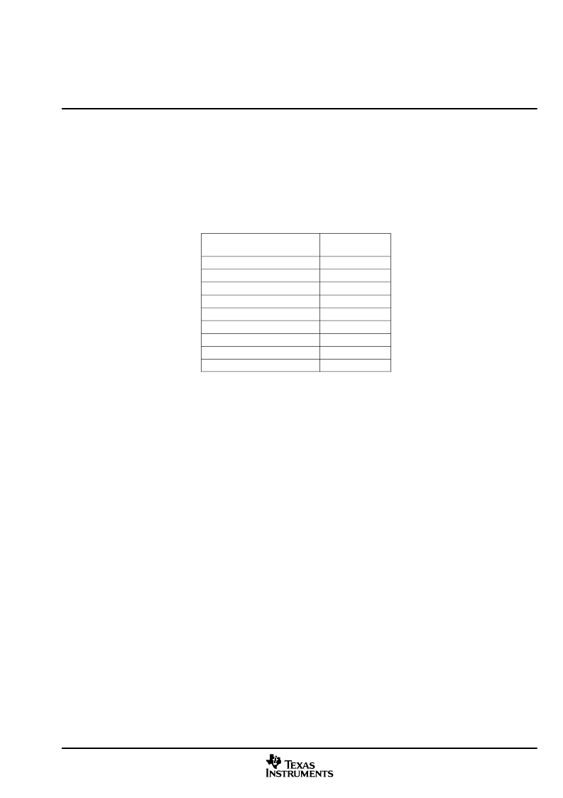
Table 1-1. Serial Data Formats
RECEIVE SERIAL DATA
INTERFACE FORMAT
WORD LENGTHS
Right justified
16
Right justified
20
Right justified
24
I2S
16
I2S
20
I2S
24
Left Justified
16
Left Justified
20
Left Justified
24
Serial data is input on SDIN1, SDIN2, SDIN3, and SDIN4. The TAS5028 accepts 32-, 38-, 44.1-, 48-, 88.2-,
96-, 176.4-, and 192-kHz serial data in 16-, 20-, or 24-bit data in left, right, and I
2
S serial data formats using
a 64-Fs SCLK clock and a 128, 192, 256, 384, 512, or 768 x Fs MCLK rates (up to a maximum of 50 MHz).
The parameters of this clock and serial data interface are I
2
C configurable.
1.4.3 I
2
C Serial Control Interface
The TAS5028 has an I
2
C serial control slave interface (address 0x36) to receive commands from a system
controller. The serial control interface supports both normal-speed (100 kHz) and high-speed (400 kHz)
operations without wait states. Since the TAS5028 has a crystal time base, this interface operates even when
MCLK is absent.
The serial control interface supports both single byte and multi-byte read / write operations for status registers
and the general control registers associated with the PWM. However, for the DAP data processing registers,
the serial control interface also supports multiple byte (4 byte) write operations.
The I
2
C supports a special mode which permits I
2
C write operations to be broken up into multiple data write
operations that are multiples of 4 data bytes. These are 6 byte, 10 byte, 14 byte, 18 byte ... etc write operations
that are composed of a device address, read/write bit, and subaddress and any multiple of 4 bytes of data.
This permits the system to incrementally write large register values without blocking other I
2
C transactions.
In order to use this feature, the first chunk of data is written to the target I
2
C address and each chunk of
subsequent data is written to a special append register (0xFE), until all the data is written and a stop bit is sent.
An incremental read operation is not supported.
1.4.4 Device Control
The TAS5028 control section provides the control and sequencing for the TAS5028. The device control
provides both high and low level control for the serial control interface, clock and serial data interfaces, digital
audio processor, and pulse width modulator sections.
1.4.5 Digital Audio Processor (DAP)
The DAP arithmetic unit is used to implement all audio processing functions – soft volume, bass and treble
processing, and input and output mixing. Figure 1-6 shows the TAS5028 DAP architecture.
相關(guān)PDF資料 |
PDF描述 |
|---|---|
| TAS5036A | Six Channel Digital Audio PWM Processor |
| TAS5036A_06 | Six Channel Digital Audio PWM Processor |
| TAS5036AIPFC | Six Channel Digital Audio PWM Processor |
| TAS5036AIPFCG4 | Six Channel Digital Audio PWM Processor |
| TAS5036AIPFCR | Six Channel Digital Audio PWM Processor |
相關(guān)代理商/技術(shù)參數(shù) |
參數(shù)描述 |
|---|---|
| TAS5036 | 制造商:TI 制造商全稱(chēng):Texas Instruments 功能描述:SIX CHANNEL DIGITAL AUDIO PWM PROCESSOR |
| TAS5036A | 制造商:TI 制造商全稱(chēng):Texas Instruments 功能描述:Six Channel Digital Audio PWM Processor |
| TAS5036A_06 | 制造商:TI 制造商全稱(chēng):Texas Instruments 功能描述:Six Channel Digital Audio PWM Processor |
| TAS5036AIPFC | 功能描述:音頻放大器 Digital Audio PWM Processor RoHS:否 制造商:STMicroelectronics 產(chǎn)品:General Purpose Audio Amplifiers 輸出類(lèi)型:Digital 輸出功率: THD + 噪聲: 工作電源電壓:3.3 V 電源電流: 最大功率耗散: 最大工作溫度: 安裝風(fēng)格:SMD/SMT 封裝 / 箱體:TQFP-64 封裝:Reel |
| TAS5036AIPFCG4 | 功能描述:音頻放大器 Digital Audio PWM Processor RoHS:否 制造商:STMicroelectronics 產(chǎn)品:General Purpose Audio Amplifiers 輸出類(lèi)型:Digital 輸出功率: THD + 噪聲: 工作電源電壓:3.3 V 電源電流: 最大功率耗散: 最大工作溫度: 安裝風(fēng)格:SMD/SMT 封裝 / 箱體:TQFP-64 封裝:Reel |
發(fā)布緊急采購(gòu),3分鐘左右您將得到回復(fù)。