- 您現(xiàn)在的位置:買賣IC網(wǎng) > PDF目錄383837 > ST16C654IJ68 (EXAR CORP) 2.97V TO 5.5V QUAD UART WITH 64-BYTE FIFO PDF資料下載
參數(shù)資料
| 型號: | ST16C654IJ68 |
| 廠商: | EXAR CORP |
| 元件分類: | 微控制器/微處理器 |
| 英文描述: | 2.97V TO 5.5V QUAD UART WITH 64-BYTE FIFO |
| 中文描述: | 4 CHANNEL(S), 1.5M bps, SERIAL COMM CONTROLLER, PQCC68 |
| 封裝: | PLASTIC, LCC-68 |
| 文件頁數(shù): | 12/51頁 |
| 文件大?。?/td> | 968K |
| 代理商: | ST16C654IJ68 |
第1頁第2頁第3頁第4頁第5頁第6頁第7頁第8頁第9頁第10頁第11頁當(dāng)前第12頁第13頁第14頁第15頁第16頁第17頁第18頁第19頁第20頁第21頁第22頁第23頁第24頁第25頁第26頁第27頁第28頁第29頁第30頁第31頁第32頁第33頁第34頁第35頁第36頁第37頁第38頁第39頁第40頁第41頁第42頁第43頁第44頁第45頁第46頁第47頁第48頁第49頁第50頁第51頁
ST16C654/654D
2.97V TO 5.5V QUAD UART WITH 64-BYTE FIFO
REV. 5.0.0
12
2.7
The 654 includes an on-chip oscillator (XTAL1 and XTAL2) to produce a clock for both UART sections in the
device. The CPU data bus does not require this clock for bus operation. The crystal oscillator provides a
system clock to the Baud Rate Generators (BRG) section found in each of the UART. XTAL1 is the input to the
oscillator or external clock buffer input with XTAL2 pin being the output. For programming details, see
“Section
2.8, Programmable Baud Rate Generator” on page 12
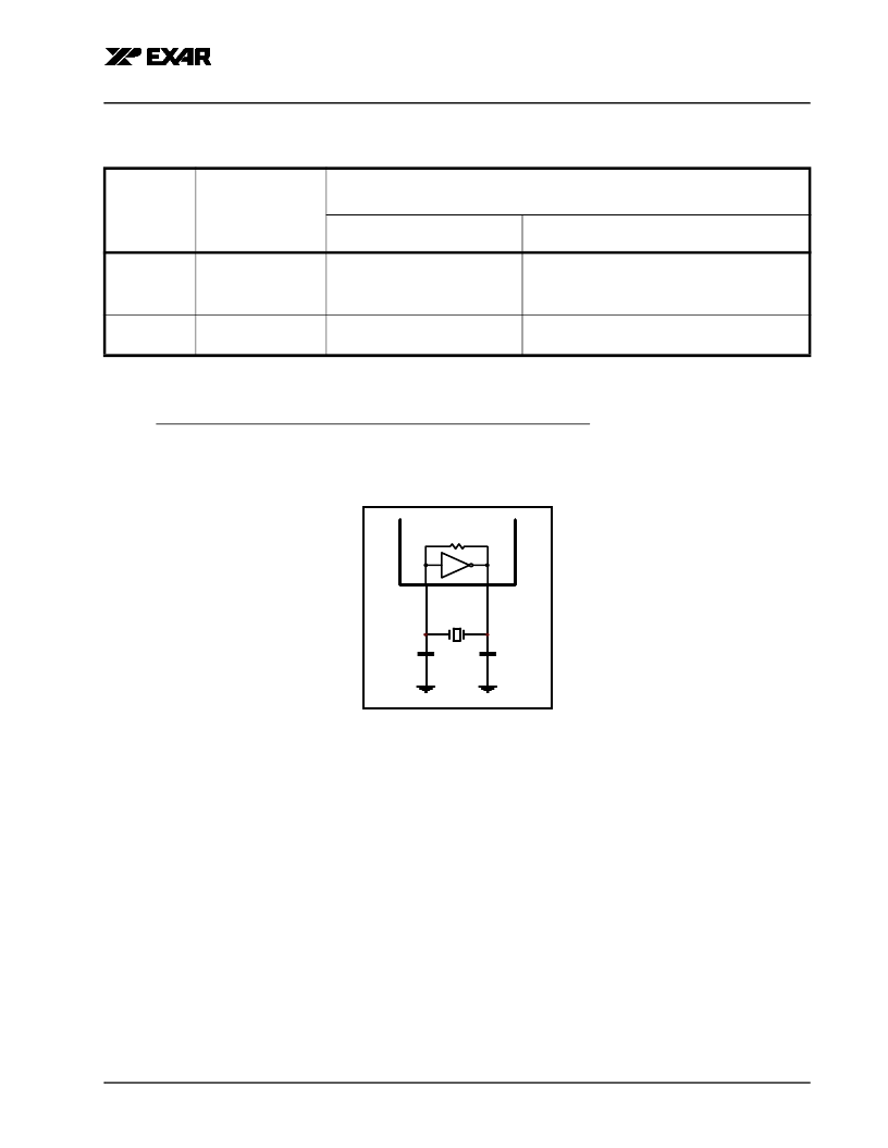
F
IGURE
5. T
YPICAL
OSCILLATOR
CONNECTIONS
Crystal Oscillator or External Clock Input
The on-chip oscillator is designed to use an industry standard microprocessor crystal (parallel resonant,
fundamental frequency with 10-22 pF capacitance load, ESR of 20-120 ohms and 100ppm frequency
tolerance) connected externally between the XTAL1 and XTAL2 pins. Typical oscillator connections are shown
in
Figure 5
. Alternatively, an external clock can be connected to the XTAL1 pin to clock the internal baud rate
generator for standard or custom rates. For further reading on oscillator circuit please see application note
DAN108 on EXAR’s web site.
2.8
Programmable Baud Rate Generator
Each UART has its own Baud Rate Generator (BRG) with a prescaler. The prescaler is controlled by a software
bit in the MCR register. The MCR register bit-7 sets the prescaler to divide the input crystal or external clock by
1 or 4. The clock output of the prescaler goes to the BRG. The BRG further divides this clock by a
programmable divisor between 1 and (2
16
-1) to obtain a 16X sampling rate clock of the serial data rate. The
sampling rate clock is used by the transmitter for data bit shifting and receiver for data sampling.
T
ABLE
5: TXRDY#
AND
RXRDY# O
UTPUTS
IN
FIFO
AND
DMA M
ODE
FOR
C
HANNELS
A-D
P
INS
FCR
BIT
-0=0
(FIFO D
ISABLED
)
FCR B
IT
-0=1 (FIFO E
NABLED
)
FCR Bit-3 = 0
(DMA Mode Disabled)
FCR Bit-3 = 1
(DMA Mode Enabled)
RXRDY#
0 = 1 byte
1 = no data
0 = at least 1 byte in FIFO
1 = FIFO empty
1 to 0 transition when FIFO reaches the trigger
level, or timeout occurs.
0 to 1 transition when FIFO empties.
TXRDY#
0 = THR empty
1 = byte in THR
0 = FIFO empty
1 = at least 1 byte in FIFO
0 = FIFO has at least 1 empty location.
1 = FIFO is full.
C1
22-47pF
C2
22-47pF
14.7456
MHz
XTAL1
XTAL2
R=300K to 400K
相關(guān)PDF資料 |
PDF描述 |
|---|---|
| ST16C654IQ100 | 2.97V TO 5.5V QUAD UART WITH 64-BYTE FIFO |
| ST16C654IQ64 | 2.97V TO 5.5V QUAD UART WITH 64-BYTE FIFO |
| ST16KF74 | Microcontroller |
| ST16LF74 | Microcontroller |
| ST16MF74 | Microcontroller |
相關(guān)代理商/技術(shù)參數(shù) |
參數(shù)描述 |
|---|---|
| ST16C654IJ68-F | 功能描述:UART 接口集成電路 QUAD UARTW/64BYTE FIFO RoHS:否 制造商:Texas Instruments 通道數(shù)量:2 數(shù)據(jù)速率:3 Mbps 電源電壓-最大:3.6 V 電源電壓-最小:2.7 V 電源電流:20 mA 最大工作溫度:+ 85 C 最小工作溫度:- 40 C 封裝 / 箱體:LQFP-48 封裝:Reel |
| ST16C654IJ68-F | 制造商:Exar Corporation 功能描述:IC QUAD UART 1.5MBPS 5.5V 68-PLCC |
| ST16C654IJ68TR-F | 制造商:Exar Corporation 功能描述:UART 4-CH 64Byte FIFO 3.3V/5V 68-Pin PLCC T/R 制造商:Exar Corporation 功能描述:2.97V to 5.5V Quad UART with 64 Byte FIFOs PLCC 68 制造商:Exar Corporation 功能描述:ST16C654IJ68TR-F |
| ST16C654IQ | 制造商:Exar Corporation 功能描述: |
| ST16C654IQ100 | 制造商:EXAR 制造商全稱:EXAR 功能描述:QUAD UART WITH 64-BYTE FIFO AND INFRARED (IrDA) ENCODER/DECODER |
發(fā)布緊急采購,3分鐘左右您將得到回復(fù)。