- 您現(xiàn)在的位置:買(mǎi)賣(mài)IC網(wǎng) > PDF目錄383827 > SP8605 12-Bit Sampling A/D Converters PDF資料下載
參數(shù)資料
| 型號(hào): | SP8605 |
| 元件分類(lèi): | 串行ADC |
| 英文描述: | 12-Bit Sampling A/D Converters |
| 中文描述: | 12位采樣的A / D轉(zhuǎn)換器 |
| 文件頁(yè)數(shù): | 7/11頁(yè) |
| 文件大?。?/td> | 205K |
| 代理商: | SP8605 |
85
INPUT VOLTAGE RANGE AND LSB VALUES
Input Voltage Range Defined As:
Analog Input Connected to Pin
Pin Connected to AGND
One Least Significant Bit (LSB)
0V to +10V
2
3
10V/2
12
2.44mV
0V to +5V
3
2
5V/2
12
1.22mV
FSR/2
12
OUTPUT TRANSITION VALUES
FFEH TO FFFH
+ FULL SCALE
+10V–3/2LSB
+9.963V
4.9988V
1.22mV
+5V–3/2LSB
+4.9982V
2.4994V
0.6mV
7FFH TO 800H
000H to 001H
Mid Scale
0V
Table 2. Input Voltages, Transition Voltages and LSB Values
FFE
H
= 4094
DEC
.
+10V Range Offset and Gain
Offset
— Apply 0.0012V to the +10V input at
pin 2. Adjust the offset potentiometer until the
LSB toggles on and off at code 0000 0000
0000
BIN
= 000
H
= 0000
DEC
.
Gain
— Apply 9.9963V to the +10V input at pin
2. Adjust the gain potentiometer until the LSB
toggles on and off at code 1111 1111 1110
BIN
=
FFE
H
= 4094
DEC
.
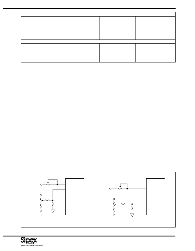
Layout Considerations
Because of the high resolution and linearity of the
SP86XX Series
, system design problems such as
ground path resistance and contact resistance become
very important.
The input resistance of the
SP86XX Series
is 6.3k
or 4.2K
(for the 10V and 5V ranges respectively).
connections as shown in
Figure 2
should be used.
Calibration Procedure
Apply a precision input voltage source to your
chosen input range (10V range at pin 2 or 5V at
pin 3). Set the A/D to convert continuously.
Monitor the output code. Trim the offset first,
then gain. Use the appropriate input voltages
and output target codes for your chosen input
range as follows. The recommended offset cali-
bration voltage values eliminate interaction be-
tween the offset and gain calibration
+5V Range Offset and Gain
Offset
— Apply 0.0006V to the +5V input at pin
3. Adjust the offset potentiometer until the LSB
toggles on and off at code 0000 0000 0000
BIN
=
000
H
= 0000
DEC
.
Gain
— Apply 4.9982V to the +5V input at pin
3. Adjust the gain potentiometer until the LSB
toggles on and off at code 1111 1111 1110
BIN
=
SP86XX
2
3
4
5
6
7
R
2
=500
+5V
+10V
Input
GAIN ADJUST
100
10K
UNIPOLAR ZERO ADJUST
R
1
=10K
6.65K
–15V
SP86XX
2
3
4
5
6
7
GAIN ADJUST
R
2
=500
+5V
+5V
Input
R
1
=10K
10K
–15V
30.1K
301
Figure 3. a) 10V Range b) 5V Range — With External Trims
a)
b)
相關(guān)PDF資料 |
PDF描述 |
|---|---|
| SPB16035 | Schottky Rectifier |
| SPB16040 | Schottky Rectifier |
| SPB16045 | Schottky Rectifier |
| SPW17N80C2 | TRANSISTOR | MOSFET | N-CHANNEL | 800V V(BR)DSS | 17A I(D) | TO-247VAR |
| SR-5R1 | ZUGENTLASTER FUER RUNDKABEL 6 BIS 7.4MM Inhalt pro Packung: 100 Stk. |
相關(guān)代理商/技術(shù)參數(shù) |
參數(shù)描述 |
|---|---|
| SP8607 | 制造商:ZARLINK 制造商全稱(chēng):Zarlink Semiconductor Inc 功能描述:emitter coupled logic divider |
| SP8607ACCM | 制造商:ZARLINK 制造商全稱(chēng):Zarlink Semiconductor Inc 功能描述:emitter coupled logic divider |
| SP8607ACM | 制造商:ZARLINK 制造商全稱(chēng):Zarlink Semiconductor Inc 功能描述:emitter coupled logic divider |
| SP8607BCM | 制造商:ZARLINK 制造商全稱(chēng):Zarlink Semiconductor Inc 功能描述:emitter coupled logic divider |
| SP-860-AR-SK | 功能描述:顯示開(kāi)發(fā)工具 Starter kit of SP-860 AR RoHS:否 制造商:4D Systems 產(chǎn)品:4Display Shields 工具用于評(píng)估:?OLED-160-G1, ?OLED-160-G2 接口類(lèi)型:Serial 工作電源電壓:5 V |
發(fā)布緊急采購(gòu),3分鐘左右您將得到回復(fù)。