- 您現(xiàn)在的位置:買賣IC網(wǎng) > PDF目錄373442 > SN54ALVTH16601WD (Texas Instruments, Inc.) 2.5-V/3.3-V 18-BIT UNIVERSAL BUS TRANSCEIVER WITH 3-STATE OUTPUTS PDF資料下載
參數(shù)資料
| 型號(hào): | SN54ALVTH16601WD |
| 廠商: | Texas Instruments, Inc. |
| 元件分類: | 通用總線功能 |
| 英文描述: | 2.5-V/3.3-V 18-BIT UNIVERSAL BUS TRANSCEIVER WITH 3-STATE OUTPUTS |
| 中文描述: | 2.5-V/3.3-V 18位通用總線收發(fā)器和三態(tài)輸出 |
| 文件頁數(shù): | 2/12頁 |
| 文件大小: | 196K |
| 代理商: | SN54ALVTH16601WD |
SN54ALVTH16601, SN74ALVTH16601
2.5-V/3.3-V 18-BIT UNIVERSAL BUS TRANSCEIVER
WITH 3-STATE OUTPUTS
SCES143A – SEPTEMBER 1998 – REVISED JULY 1999
2
POST OFFICE BOX 655303
DALLAS, TEXAS 75265
description (continued)
Data flow in each direction is controlled by output-enable (OEAB and OEBA), latch-enable (LEAB and LEBA),
and clock (CLKAB and CLKBA) inputs. The clock can be controlled by the clock-enable (CLKENAB and
CLKENBA) inputs. For A-to-B data flow, the device operates in the transparent mode when LEAB is high. When
LEAB is low, the A data is latched if CLKAB is held at a high or low logic level. If LEAB is low, the A data is stored
in the latch/flip-flop on the low-to-high transition of CLKAB. Output enable OEAB is active low. When OEAB is
low, the outputs are active. When OEAB is high, the outputs are in the high-impedance state.
Data flow for B to A is similar to that of A to B, but uses OEBA, LEBA, CLKBA, and CLKENBA.
This device is fully specified for hot-insertion applications using I
off
and power-up 3-state. The I
off
circuitry
disables the outputs, preventing damaging current backflow through the device when it is powered down. The
power-up 3-state circuitry places the outputs in the high-impedance state during power up and power down,
which prevents driver conflict.
When V
CC
is between 0 and 1.2 V, the device is in the high-impedance state during power up or power down.
However, to ensure the high-impedance state above 1.2 V, OE should be tied to V
CC
through a pullup resistor;
the minimum value of the resistor is determined by the current-sinking capability of the driver.
Active bus-hold circuitry is provided to hold unused or floating data inputs at a valid logic level.
The SN54ALVTH16601 is characterized for operation over the full military temperature range of –55
°
C to
125
°
C. The SN74ALVTH16601 is characterized for operation from –40
°
C to 85
°
C.
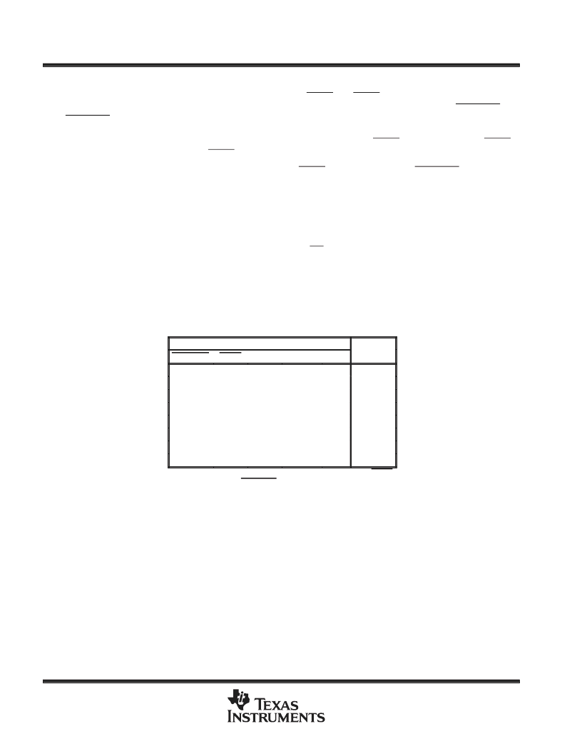
FUNCTION TABLE
INPUTS
OUTPUT
B
CLKENAB
X
OEAB
H
LEAB
X
CLKAB
A
X
X
Z
X
L
H
X
L
L
X
L
H
X
H
H
H
L
L
X
X
B0
B0
L
H
L
L
X
↑
↑
X
L
L
L
L
L
L
L
H
H
L
L
L
L or H
X
B0
A-to-B data flow is shown: B-to-A flow is similar but uses OEBA,
LEBA, CLKBA, and CLKENBA.
Output level before the indicated steady-state input conditions were
established
相關(guān)PDF資料 |
PDF描述 |
|---|---|
| SN74ALVTH16601DGG | 2.5-V/3.3-V 18-BIT UNIVERSAL BUS TRANSCEIVER WITH 3-STATE OUTPUTS |
| SN74ALVTH16601DGV | 2.5-V/3.3-V 18-BIT UNIVERSAL BUS TRANSCEIVER WITH 3-STATE OUTPUTS |
| SN54ALVTH16646 | 2.5-V/3.3-V 16-Bit Bus Transceivers With 3-State Outputs( 2.5V/3.3V 16位總線收發(fā)器(三態(tài)輸出)) |
| SN74ALVTH16646 | 2.5-V/3.3-V 16-Bit Bus Transceivers With 3-State Outputs( 2.5V/3.3V16位總線收發(fā)器(三態(tài)輸出)) |
| SN54ALVTH16821WD | 2.5-V/3.3-V 20-BIT BUS-INTERFACE FLIP-FLOPS WITH 3-STATE OUTPUTS |
相關(guān)代理商/技術(shù)參數(shù) |
參數(shù)描述 |
|---|---|
| SN54AS00J | 制造商:Texas Instruments 功能描述:QUAD 2-INPUT NAND GATE - Rail/Tube |
| SN54AS04J | 制造商:Texas Instruments 功能描述:HEX INVERTER - Rail/Tube |
| SN54AS08J | 制造商:Texas Instruments 功能描述:AND Gate 4-Element 2-IN Bipolar 14-Pin CDIP Tube 制造商:Texas Instruments 功能描述:AND GATE 4-ELEM 2-IN BIPOLAR 14CDIP - Rail/Tube |
| SN54AS08W | 制造商:Texas Instruments 功能描述: |
| SN54AS1004AJ | 制造商:Texas Instruments 功能描述:Driver 6-CH Inverting Bipolar 14-Pin CDIP Tube |
發(fā)布緊急采購,3分鐘左右您將得到回復(fù)。