- 您現(xiàn)在的位置:買賣IC網(wǎng) > PDF目錄385811 > S75PL127J (Spansion Inc.) Power supply woltage of 2.7 to 3.1 volt PDF資料下載
參數(shù)資料
| 型號(hào): | S75PL127J |
| 廠商: | Spansion Inc. |
| 英文描述: | Power supply woltage of 2.7 to 3.1 volt |
| 中文描述: | 功率2月7號(hào)至三月一日伏的電源woltage |
| 文件頁(yè)數(shù): | 58/183頁(yè) |
| 文件大小: | 1409K |
| 代理商: | S75PL127J |
第1頁(yè)第2頁(yè)第3頁(yè)第4頁(yè)第5頁(yè)第6頁(yè)第7頁(yè)第8頁(yè)第9頁(yè)第10頁(yè)第11頁(yè)第12頁(yè)第13頁(yè)第14頁(yè)第15頁(yè)第16頁(yè)第17頁(yè)第18頁(yè)第19頁(yè)第20頁(yè)第21頁(yè)第22頁(yè)第23頁(yè)第24頁(yè)第25頁(yè)第26頁(yè)第27頁(yè)第28頁(yè)第29頁(yè)第30頁(yè)第31頁(yè)第32頁(yè)第33頁(yè)第34頁(yè)第35頁(yè)第36頁(yè)第37頁(yè)第38頁(yè)第39頁(yè)第40頁(yè)第41頁(yè)第42頁(yè)第43頁(yè)第44頁(yè)第45頁(yè)第46頁(yè)第47頁(yè)第48頁(yè)第49頁(yè)第50頁(yè)第51頁(yè)第52頁(yè)第53頁(yè)第54頁(yè)第55頁(yè)第56頁(yè)第57頁(yè)當(dāng)前第58頁(yè)第59頁(yè)第60頁(yè)第61頁(yè)第62頁(yè)第63頁(yè)第64頁(yè)第65頁(yè)第66頁(yè)第67頁(yè)第68頁(yè)第69頁(yè)第70頁(yè)第71頁(yè)第72頁(yè)第73頁(yè)第74頁(yè)第75頁(yè)第76頁(yè)第77頁(yè)第78頁(yè)第79頁(yè)第80頁(yè)第81頁(yè)第82頁(yè)第83頁(yè)第84頁(yè)第85頁(yè)第86頁(yè)第87頁(yè)第88頁(yè)第89頁(yè)第90頁(yè)第91頁(yè)第92頁(yè)第93頁(yè)第94頁(yè)第95頁(yè)第96頁(yè)第97頁(yè)第98頁(yè)第99頁(yè)第100頁(yè)第101頁(yè)第102頁(yè)第103頁(yè)第104頁(yè)第105頁(yè)第106頁(yè)第107頁(yè)第108頁(yè)第109頁(yè)第110頁(yè)第111頁(yè)第112頁(yè)第113頁(yè)第114頁(yè)第115頁(yè)第116頁(yè)第117頁(yè)第118頁(yè)第119頁(yè)第120頁(yè)第121頁(yè)第122頁(yè)第123頁(yè)第124頁(yè)第125頁(yè)第126頁(yè)第127頁(yè)第128頁(yè)第129頁(yè)第130頁(yè)第131頁(yè)第132頁(yè)第133頁(yè)第134頁(yè)第135頁(yè)第136頁(yè)第137頁(yè)第138頁(yè)第139頁(yè)第140頁(yè)第141頁(yè)第142頁(yè)第143頁(yè)第144頁(yè)第145頁(yè)第146頁(yè)第147頁(yè)第148頁(yè)第149頁(yè)第150頁(yè)第151頁(yè)第152頁(yè)第153頁(yè)第154頁(yè)第155頁(yè)第156頁(yè)第157頁(yè)第158頁(yè)第159頁(yè)第160頁(yè)第161頁(yè)第162頁(yè)第163頁(yè)第164頁(yè)第165頁(yè)第166頁(yè)第167頁(yè)第168頁(yè)第169頁(yè)第170頁(yè)第171頁(yè)第172頁(yè)第173頁(yè)第174頁(yè)第175頁(yè)第176頁(yè)第177頁(yè)第178頁(yè)第179頁(yè)第180頁(yè)第181頁(yè)第182頁(yè)第183頁(yè)
August 12, 2004 S29PL127J_064J_032J_MCP_00_A3
S29PL127J/S29PL064J/S29PL032J for MCP
59
P r e l i m i n a r y
Absolute Maximum Ratings
Storage Temperature Plastic Packages . . . . . . . . . . . . . . . . .–65°C to +150°C
Ambient Temperature with Power Applied. . . . . . . . . . . . . . .–65°C to +125°C
Voltage with Respect to Ground
V
CC
(Note 1). . . . . . . . . . . . . . . . . . . . . . . . . . . . . . . . . . . –0.5 V to +4.0 V
RESET# (Note 2) . . . . . . . . . . . . . . . . . . . . . . . . . . . . . . –0.5 V to +13.0 V
WP#/ACC (Note 2) . . . . . . . . . . . . . . . . . . . . . . . . . . . . . –0.5 V to +10.5 V
All other pins (Note 1) . . . . . . . . . . . . . . . . . . . . . . . . . –0.5 V to V
CC
+0.5 V
Output Short Circuit Current (Note 3) . . . . . . . . . . . . . . . . . . . . . . . 200 mA
Notes:
1. Minimum DC voltage on input or I/O pins is –0.5 V. During voltage transitions,
input or I/O pins may overshoot V
SS
to –2.0 V for periods of up to 20 ns. Maximum
DC voltage on input or I/O pins is V
CC
+ 0.5 V. During voltage transitions, input or
I/O pins may overshoot to V
CC
+ 2.0 V for periods up to 20 ns. See
Figure 8
.
2. Minimum DC input voltage on pins A9, OE#, RESET#, and WP#/ACC is –0.5 V.
During voltage transitions, A9, OE#, WP#/ACC, and RESET# may overshoot V
SS
to –2.0 V for periods of up to 20 ns. See
Figure 8
. Maximum DC input voltage on
pin A9, OE#, and RESET# is + 12.5 V which may overshoot to + 14.0 V for periods
up to 20 ns. Maximum DC input voltage on WP#/ACC is + 9.5 V which may
overshoot to + 12.0 V for periods up to 20 ns.
3. No more than one output may be shorted to ground at a time. Duration of the
short circuit should not be greater than one second.
4. Stresses above those listed under “Absolute Maximum Ratings” may cause perma-
nent damage to the device. This is a stress rating only; functional operation of the
device at these or any other conditions above those indicated in the operational
sections of this data sheet is not implied. Exposure of the device to absolute max-
imum rating conditions for extended periods may affect device reliability.
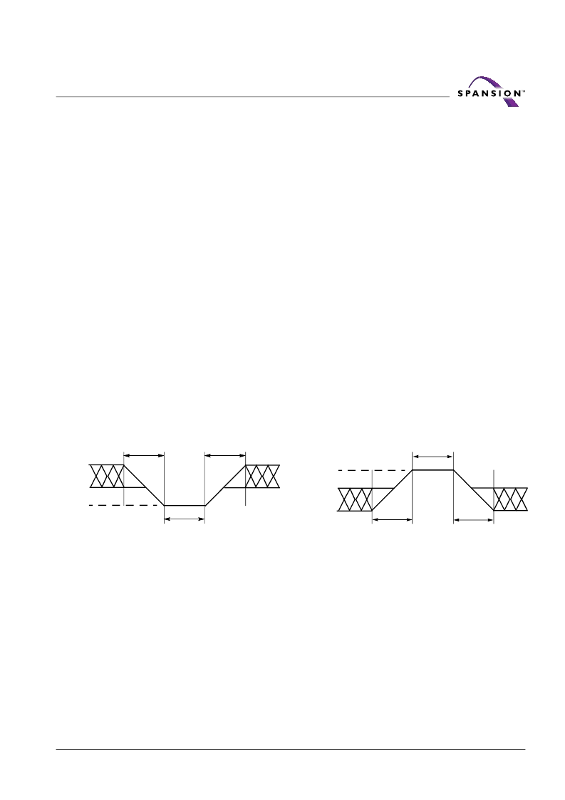
Figure 8. Maximum Overshoot Waveforms
20 ns
20 ns
+0.8 V
–0.5 V
20 ns
–2.0 V
20 ns
20 ns
V
CC
+2.0 V
V
CC
+0.5 V
20 ns
2.0 V
Maximum Negative Overshoot Waveform
Maximum Positive Overshoot Waveform
相關(guān)PDF資料 |
PDF描述 |
|---|---|
| S75PL127JCEBFWU0 | Power supply woltage of 2.7 to 3.1 volt |
| S75PL127JCFBFWB2 | Power supply woltage of 2.7 to 3.1 volt |
| S7AH-06E | NON-ISOLATED DC/DC CONVERTERS 4.5 13.2V Input / 1.0 ? 3.3V Output / 6A |
| S7AH-08B250 | NON-ISOLATED DC/DC CONVERTERS 5V Input / 0.9V - 3.3V Output / 8A |
| S7AH-08B330 | NON-ISOLATED DC/DC CONVERTERS 5V Input / 0.9V - 3.3V Output / 8A |
相關(guān)代理商/技術(shù)參數(shù) |
參數(shù)描述 |
|---|---|
| S75PL127JBD | 制造商:SPANSION 制造商全稱:SPANSION 功能描述:Power supply woltage of 2.7 to 3.1 volt |
| S75PL127JBDBAWB0 | 制造商:SPANSION 制造商全稱:SPANSION 功能描述:Power supply woltage of 2.7 to 3.1 volt |
| S75PL127JBDBAWB2 | 制造商:SPANSION 制造商全稱:SPANSION 功能描述:Power supply woltage of 2.7 to 3.1 volt |
| S75PL127JBDBAWB3 | 制造商:SPANSION 制造商全稱:SPANSION 功能描述:Power supply woltage of 2.7 to 3.1 volt |
| S75PL127JBDBAWU0 | 制造商:SPANSION 制造商全稱:SPANSION 功能描述:Power supply woltage of 2.7 to 3.1 volt |
發(fā)布緊急采購(gòu),3分鐘左右您將得到回復(fù)。