- 您現(xiàn)在的位置:買賣IC網(wǎng) > PDF目錄225025 > RC28F128P33T85 (NUMONYX) 8M X 16 FLASH 3V PROM, 85 ns, PBGA64 PDF資料下載
參數(shù)資料
| 型號: | RC28F128P33T85 |
| 廠商: | NUMONYX |
| 元件分類: | PROM |
| 英文描述: | 8M X 16 FLASH 3V PROM, 85 ns, PBGA64 |
| 封裝: | BGA-64 |
| 文件頁數(shù): | 53/96頁 |
| 文件大?。?/td> | 1378K |
| 代理商: | RC28F128P33T85 |
第1頁第2頁第3頁第4頁第5頁第6頁第7頁第8頁第9頁第10頁第11頁第12頁第13頁第14頁第15頁第16頁第17頁第18頁第19頁第20頁第21頁第22頁第23頁第24頁第25頁第26頁第27頁第28頁第29頁第30頁第31頁第32頁第33頁第34頁第35頁第36頁第37頁第38頁第39頁第40頁第41頁第42頁第43頁第44頁第45頁第46頁第47頁第48頁第49頁第50頁第51頁第52頁當(dāng)前第53頁第54頁第55頁第56頁第57頁第58頁第59頁第60頁第61頁第62頁第63頁第64頁第65頁第66頁第67頁第68頁第69頁第70頁第71頁第72頁第73頁第74頁第75頁第76頁第77頁第78頁第79頁第80頁第81頁第82頁第83頁第84頁第85頁第86頁第87頁第88頁第89頁第90頁第91頁第92頁第93頁第94頁第95頁第96頁
November 2007
Datasheet
Order Number: 314749-05
57
Numonyx StrataFlash Embedded Memory (P33)
11.2.4
CFI Query
The CFI Query command instructs the device to output Common Flash Interface (CFI)
data when read. See Section 9.6, “Device Command Bus Cycles” on page 44 for details
on issuing the CFI Query command. Appendix , “Common Flash Interface” on page 77
shows CFI information and address offsets within the CFI database.
11.3
Programming Operations
The device supports three programming methods: Word Programming (40h/10h),
Buffered Programming (E8h, D0h), and Buffered Enhanced Factory Programming (80h,
D0h). The following sections describe device programming in detail.
Successful programming requires the addressed block to be unlocked. If the block is
locked down, WP# must be deasserted and the block must be unlocked before
attempting to program the block. Attempting to program a locked block causes a
program error (SR[4] and SR[1] set) and termination of the operation. See Section
11.4.5, “Security Modes” on page 64 for details on locking and unlocking blocks.
The Numonyx StrataFlash Embedded Memory (P33) is segmented into multiple 8-
Mbit Programming Regions. See Section 4.4, “Memory Maps” on page 22 for complete
addressing. Execute in Place (XIP) applications must partition the memory such that
code and data are in separate programming regions. XIP is executing code directly
from flash memory. Each Programming Region should contain only code or data but not
both. The following terms define the difference between code and data. System designs
must use these definitions when partitioning their code and data for the Numonyx
StrataFlash Embedded Memory (P33) device.
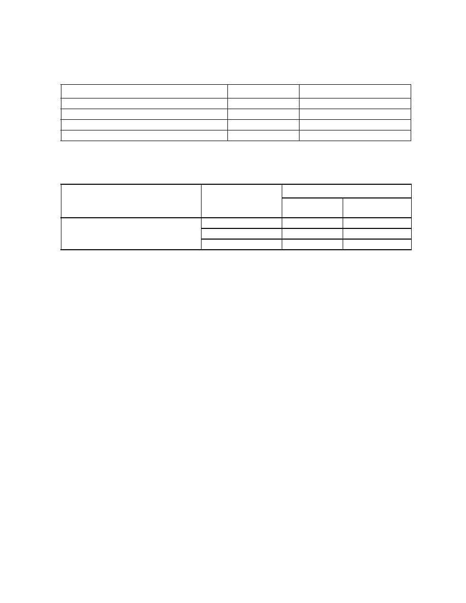
64-bit Factory-Programmed Protection Register
0x81–0x84
Factory Protection Register Data
64-bit User-Programmable Protection Register
0x85–0x88
User Protection Register Data
Lock Register 1
0x89
Protection Register Lock Data
128-bit User-Programmable Protection Registers
0x8A–0x109
PR-LK1
Notes:
1.
BBA = Block Base Address.
Table 31: Device ID codes
ID Code Type
Device Density
Device Identifier Codes
–T
(Top Parameter)
–B
(Bottom Parameter)
Device Code
64-Mbit
881D
8820
128-Mbit
881E
8821
256-Mbit
891F
8922
Note:
The 512-Mbit devices do not have a Device ID associated with them. Each die within the stack can be identified by either
of the 256-Mbit Device ID codes depending on its parameter option.
Table 30: Device Identifier Information (Sheet 2 of 2)
Item
Address(1)
Data
Code :
Execution code ran out of the flash device on a continuous basis in the system.
Data :
Information periodically programmed into the flash device and read back (e.g. execution code
shadowed and executed in RAM, pictures, log files, etc.).
相關(guān)PDF資料 |
PDF描述 |
|---|---|
| RC28F256P33T85A | 16M X 16 FLASH 3V PROM, 85 ns, PBGA64 |
| RC28F160C3TC90 | 1M X 16 FLASH 3V PROM, 90 ns, PBGA64 |
| RC28F160C3BD70 | 1M X 16 FLASH 3V PROM, 70 ns, PBGA64 |
| RC4194K | DUAL OUTPUT, ADJUSTABLE MIXED REGULATOR, MBFM9 |
| RM4194K | DUAL OUTPUT, ADJUSTABLE MIXED REGULATOR, MBFM9 |
相關(guān)代理商/技術(shù)參數(shù) |
參數(shù)描述 |
|---|---|
| RC28F128P33T85A | 功能描述:IC FLASH 128MBIT 85NS 64EZBGA RoHS:否 類別:集成電路 (IC) >> 存儲器 系列:StrataFlash™ 標(biāo)準(zhǔn)包裝:2,500 系列:- 格式 - 存儲器:EEPROMs - 串行 存儲器類型:EEPROM 存儲容量:1K (128 x 8) 速度:100kHz 接口:UNI/O?(單線) 電源電壓:1.8 V ~ 5.5 V 工作溫度:-40°C ~ 85°C 封裝/外殼:8-TSSOP,8-MSOP(0.118",3.00mm 寬) 供應(yīng)商設(shè)備封裝:8-MSOP 包裝:帶卷 (TR) |
| RC28F128P33TF60 | 制造商:NUMONYX 制造商全稱:Numonyx B.V 功能描述:Numonyx?? P33-65nm Flash Memory |
| RC28F128P33TF60A | 功能描述:IC FLASH 128MBIT 85NS 64EZBGA RoHS:否 類別:集成電路 (IC) >> 存儲器 系列:StrataFlash™ 標(biāo)準(zhǔn)包裝:72 系列:- 格式 - 存儲器:RAM 存儲器類型:SRAM - 同步 存儲容量:4.5M(256K x 18) 速度:133MHz 接口:并聯(lián) 電源電壓:3.135 V ~ 3.465 V 工作溫度:0°C ~ 70°C 封裝/外殼:100-LQFP 供應(yīng)商設(shè)備封裝:100-TQFP(14x20) 包裝:托盤 |
| RC28F128P3GB850 | 制造商:Micron Technology Inc 功能描述:128MB, KEARNY EBGA 3.0 - Trays |
| RC28F128P3GT850 | 制造商:Micron Technology Inc 功能描述:128MB, KEARNY EBGA 3.0 - Trays |
發(fā)布緊急采購,3分鐘左右您將得到回復(fù)。