- 您現(xiàn)在的位置:買賣IC網(wǎng) > PDF目錄299640 > PDM41258SA7SO 64K X 4 STANDARD SRAM, 7 ns, PDSO24 PDF資料下載
參數(shù)資料
| 型號(hào): | PDM41258SA7SO |
| 元件分類: | SRAM |
| 英文描述: | 64K X 4 STANDARD SRAM, 7 ns, PDSO24 |
| 文件頁(yè)數(shù): | 2/8頁(yè) |
| 文件大小: | 353K |
| 代理商: | PDM41258SA7SO |
PDM41258
2
Rev. 2.2 - 4/27/98
Absolute Maximum Ratings (1)
NOTE: 1. Stresses greater than those listed under ABSOLUTE MAXIMUM RATINGS may
cause permanent damage to the device. This is a stress rating only and functional
operation of the device at these or any other conditions above those indicated in the
operational sections of this specication is not implied. Exposure to absolute maxi-
mum rating conditions for extended periods may affect reliability
.2. Appropriate thermal calculations should be performed in all cases and specically for
those where the chosen package has a large thermal resistance (e.g., TSOP). The
calculation should be of the form: Tj = Ta + P * θja, where Ta is the ambient tempera-
ture, P is average operating power and
θ
ja the thermal resistance of the package. For
this product, use the following
θ
ja value:
SOJ: 83o C/W
Symbol
Rating
Com’l.
Ind.
Unit
TTERM
Terminal Voltage with Respect to VSS
–0.5 to +7.0
°C
TBIAS
Temperature Under Bias
–55 to +125
–65 to +135
°C
TSTG
Storage Temperature
–55 to +125
–65 to +150
°C
PT
Power Dissipation
1.0
W
IOUT
DC Output Current
50
mA
Tj
Maximum Junction Temperature (2)
125
145
°C
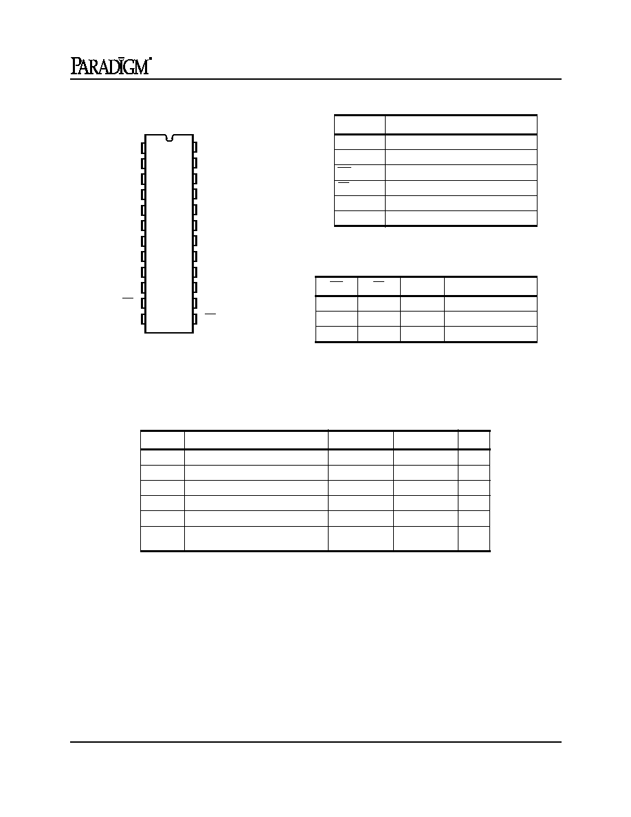
1
2
3
4
5
6
7
8
9
10
11
12
13
14
15
16
17
18
19
20
21
22
23
24
A0
A1
A2
A3
A4
A5
A6
A7
A8
A9
CE
Vss
Vcc
A15
A14
A13
A12
A11
A10
I/O3
I/O2
I/O1
I/O0
WE
Pin Conguration
SOJ
Pin Description
Name
Description
A15-A0
Address Inputs
I/O3-I/O0
Data Inputs and Outputs
WE
Write Enable Input
CE
Chip Enable Input
VCC
Power (+5V)
VSS
Ground
Truth Table
NOTE:1.H = VIH, L = VIL, X = DON’T CARE
WE
CE
I/O
MODE
X
H
Hi-Z
Standby
HL
DOUT
Read
LL
DIN
Write
相關(guān)PDF資料 |
PDF描述 |
|---|---|
| PDM41298SA20TI | 64K X 4 STANDARD SRAM, 20 ns, PDSO28 |
| PDM42245L25GI | 4K X 18 OTHER FIFO, CPGA68 |
| PDM44068SA5JI | 64K X 18 CACHE SRAM, PQCC52 |
| PDSP16350/B0/AC | 34-BIT, DSP-NUM CONTROLLED OSCILLATOR, CPGA84 |
| PDSP16488AMAACBR | 16-BIT, DSP-CONVOLVER, CPGA84 |
相關(guān)代理商/技術(shù)參數(shù) |
參數(shù)描述 |
|---|---|
| PDM41258SA8SO | 制造商:未知廠家 制造商全稱:未知廠家 功能描述:x4 SRAM |
| PDM41258SA8SOI | 制造商:未知廠家 制造商全稱:未知廠家 功能描述:x4 SRAM |
| PDM41298LA10DI | 制造商:未知廠家 制造商全稱:未知廠家 功能描述:x4 SRAM |
| PDM41298LA10P | 制造商:未知廠家 制造商全稱:未知廠家 功能描述:x4 SRAM |
| PDM41298LA10PI | 制造商:未知廠家 制造商全稱:未知廠家 功能描述:x4 SRAM |
發(fā)布緊急采購(gòu),3分鐘左右您將得到回復(fù)。