- 您現(xiàn)在的位置:買賣IC網(wǎng) > PDF目錄383735 > PAC7111 (飛思卡爾半導(dǎo)體(中國)有限公司) Microcontroller Family Hardware Specifications PDF資料下載
參數(shù)資料
| 型號(hào): | PAC7111 |
| 廠商: | 飛思卡爾半導(dǎo)體(中國)有限公司 |
| 英文描述: | Microcontroller Family Hardware Specifications |
| 中文描述: | 微控制器系列硬件規(guī)格 |
| 文件頁數(shù): | 6/56頁 |
| 文件大小: | 471K |
| 代理商: | PAC7111 |
第1頁第2頁第3頁第4頁第5頁當(dāng)前第6頁第7頁第8頁第9頁第10頁第11頁第12頁第13頁第14頁第15頁第16頁第17頁第18頁第19頁第20頁第21頁第22頁第23頁第24頁第25頁第26頁第27頁第28頁第29頁第30頁第31頁第32頁第33頁第34頁第35頁第36頁第37頁第38頁第39頁第40頁第41頁第42頁第43頁第44頁第45頁第46頁第47頁第48頁第49頁第50頁第51頁第52頁第53頁第54頁第55頁第56頁
MAC7100 Microcontroller Family Hardware Specifications, Rev. 1.2
Preliminary
Electrical Characteristics
Freescale Semiconductor
6
3.4
Operating Conditions
Unless otherwise noted, the following conditions apply to all parametric data. Refer to the temperature
rating of the device (C, V, M) with respect to ambient temperature (T
A
) and junction temperature (T
J
). For
power dissipation calculations refer to
Section 3.6, “Power Dissipation and Thermal Characteristics.”
3.4.1
Input/Output Pins
The I/O pins operate at a nominal level of 3.3 V to 5 V. This class of pins is comprised of the clocks, control
and general purpose/peripheral pins. The internal structure of these pins is identical; however, some
functionality may be disabled (for example, for analog inputs the output drivers, pull-up/down resistors
are permanently disabled).
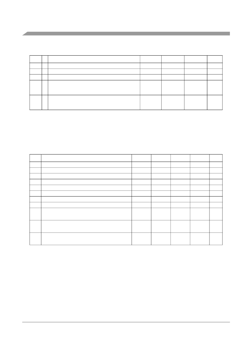
Table 6. ESD and Latch-Up Protection Characteristics
Num
C
Rating
Symbol
Min
Max
Unit
B1
B2
B3
B4
C Human Body Model (HBM)
C Machine Model (MM)
C Charge Device Model (CDM)
C Latch-up Current at T
A
= 125
°
C
positive
negative
C Latch-up Current at T
A
= 27
°
C
positive
negative
V
HBM
V
MM
V
CDM
I
LAT
2000
200
500
—
—
—
V
V
V
+100
–100
—
mA
B5
I
LAT
+200
–200
—
mA
Table 7. MAC7100 Family Device Operating Conditions
Num
Rating
Symbol
Min
Typ
Max
Unit
C1
C2
C3
C4
C5
C6
C7
C8
C9a MAC71xxC
C9b
I/O Drivers Supply Voltage
Digital Logic Supply Voltage
1
PLL Supply Voltage
1
Analog Supply Voltage
Voltage Difference V
DD
X to V
DD
A
Voltage Difference V
SS
X to V
SS
A
Oscillator Frequency
System Clock Frequency
Operating Junction Temperature Range
3
Operating Ambient Temperature Range
3
Operating Junction Temperature Range
3
Operating Ambient Temperature Range
3
Operating Junction Temperature Range
3
Operating Ambient Temperature Range
3
V
DD
X
V
DD
2.5
V
DD
PLL
V
DD
A
Δ
VDD
X
Δ
VSS
X
f
OSC
2
f
SYS
2
T
J
T
A
T
J
T
A
T
J
T
A
3.15
2.35
2.35
3.15
–0.1
–0.1
0.5
0.5
–40
–40
5
5.5
2.75
2.75
5.5
0.1
0.1
16
50
110
85
V
V
V
V
V
V
NOTES:
1. These ratings apply only when the VREG is disabled and the device is powered from an external source.
2. Throughout this document, t
OSC
refers to 1
÷
f
OSC
, and t
SYS
refers to 1
÷
f
SYS
.
3. Refer to
Section 3.6, “Power Dissipation and Thermal Characteristics,”
for more details about the relation between
ambient temperature T
A
and device junction temperature T
J
.
2.5
2.5
5
0
0
—
—
—
25
MHz
MHz
°
C
°
C
C10a MAC71xxV
C10b
–40
–40
—
25
130
105
°
C
°
C
C11a MAC71xxM
C11b
–40
–40
—
25
150
125
°
C
°
C
相關(guān)PDF資料 |
PDF描述 |
|---|---|
| PAC7112 | Microcontroller Family Hardware Specifications |
| PAC7116 | Microcontroller Family Hardware Specifications |
| PAC7121 | Microcontroller Family Hardware Specifications |
| PAC7122 | Microcontroller Family Hardware Specifications |
| PAC7126 | Microcontroller Family Hardware Specifications |
相關(guān)代理商/技術(shù)參數(shù) |
參數(shù)描述 |
|---|---|
| PAC7112 | 制造商:FREESCALE 制造商全稱:Freescale Semiconductor, Inc 功能描述:Microcontroller Family Hardware Specifications |
| PAC7116 | 制造商:FREESCALE 制造商全稱:Freescale Semiconductor, Inc 功能描述:Microcontroller Family Hardware Specifications |
| PAC7121 | 制造商:FREESCALE 制造商全稱:Freescale Semiconductor, Inc 功能描述:Microcontroller Family Hardware Specifications |
| PAC7122 | 制造商:FREESCALE 制造商全稱:Freescale Semiconductor, Inc 功能描述:Microcontroller Family Hardware Specifications |
| PAC7126 | 制造商:FREESCALE 制造商全稱:Freescale Semiconductor, Inc 功能描述:Microcontroller Family Hardware Specifications |
發(fā)布緊急采購,3分鐘左右您將得到回復(fù)。