- 您現(xiàn)在的位置:買賣IC網(wǎng) > PDF目錄383735 > PAC7111 (飛思卡爾半導(dǎo)體(中國)有限公司) Microcontroller Family Hardware Specifications PDF資料下載
參數(shù)資料
| 型號(hào): | PAC7111 |
| 廠商: | 飛思卡爾半導(dǎo)體(中國)有限公司 |
| 英文描述: | Microcontroller Family Hardware Specifications |
| 中文描述: | 微控制器系列硬件規(guī)格 |
| 文件頁數(shù): | 18/56頁 |
| 文件大?。?/td> | 471K |
| 代理商: | PAC7111 |
第1頁第2頁第3頁第4頁第5頁第6頁第7頁第8頁第9頁第10頁第11頁第12頁第13頁第14頁第15頁第16頁第17頁當(dāng)前第18頁第19頁第20頁第21頁第22頁第23頁第24頁第25頁第26頁第27頁第28頁第29頁第30頁第31頁第32頁第33頁第34頁第35頁第36頁第37頁第38頁第39頁第40頁第41頁第42頁第43頁第44頁第45頁第46頁第47頁第48頁第49頁第50頁第51頁第52頁第53頁第54頁第55頁第56頁
MAC7100 Microcontroller Family Hardware Specifications, Rev. 1.2
Preliminary
Electrical Characteristics
Freescale Semiconductor
18
3.8.3
PLL Characteristics
3.8.4
Crystal Monitor Time-out
The time-out
Table 21
shows the delay for the crystal monitor to trigger when the clock stops, either at the high
or at the low level. The corresponding clock period with an ideal 50% duty cycle is twice this time-out value.
3.8.5
Clock Quality Checker
The timing for the clock quality check is derived from the oscillator and the VCO frequency range in
Table 20
. These numbers define the upper time limit for the individual check windows to complete.
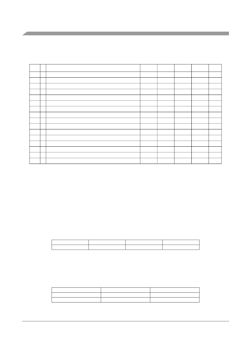
Table 20. PLL Characteristics
Num C
Rating
Symbol
Min
Typ
Max
Unit
K1
K2
K3
K4
K5
K6
K7
K8
K9
K10
K11
K12
K13
K14
K15
K16
PLL reference frequency, crystal oscillator range
P Self Clock Mode frequency
D VCO locking range
D
Lock Detector transition from Acquisition to Tracking mode
D Lock Detection
D Un-Lock Detection
D
Lock Detector transition from Tracking to Acquisition mode
C PLLON Total Stabilization delay (Auto Mode)
3
D PLLON Acquisition mode stabilization delay
3
D PLLON Tracking mode stabilization delay
3
D Charge pump current acquisition mode
D Charge pump current tracking mode
D Jitter fit VCO loop gain parameter
D Jitter fit VCO loop frequency parameter
C Jitter fit parameter 1
C Jitter fit parameter 2
f
REF
f
SCM
f
VCO
1
|Δ
trk
|
|Δ
Lock
|
|Δ
unl
|
|Δ
unt
|
t
stab
t
acq
t
al
|
i
ch
|
|
i
ch
|
K
1
f
1
j
1
j
2
0.5
2
8
3
0
0.5
6
—
—
—
—
—
—
—
—
—
—
—
—
—
—
—
—
16
5.5
50
4
1.5
2.5
8
3
5
1
5
2
5
—
—
—
—
1.3
0.12
MHz
MHz
MHz
%
2
%
2
%
2
%
2
ms
ms
ms
μ
A
μ
A
MHz/V
MHz
%
4
%
4
NOTES:
1. If CLKSEL[PLLSEL] is set then the system clock (
f
SYS
) is equal to
f
VCO
, otherwise it is equal to
f
OSC
(table
Table 19
,
J1a
or
J1b
). Throughout this document, t
SYS
is used to specify a unit of time equal to 1
÷
f
SYS
.
2. Percentage deviation from target frequency
3. PLL stabilization delay is highly dependent on operational requirement and external component values (for
example, crystal and XFC filter component values). Notes
4
and
5
show component values for a typical
configurations. Appropriate XFC filter values should be chosen based on operational requirement of system.
4.
f
OSC
= 4 MHz,
f
VCO
= 40 MHz (REFDV = 0x00, SYNR = 0x04), C
S
= 2.2 nF, C
P
= 220 pF, R
S
= 5.6 K
Ω
.
5.
f
OSC
= 4 MHz,
f
VCO
= 16 MHz (REFDV = 0x00, SYNR = 0x01), C
S
= 4.7 nF, C
P
= 470 pF, R
S
= 2.7 K
Ω
.
0.5
4
0.3
4
0.2
4
38.5
3.5
–195
126
—
—
Table 21. Crystal Monitor Time-Outs
Min
6
Typ
10
Max
18.5
Unit
μ
s
Table 22. CRG Maximum Clock Quality Check Timings
Clock Check Windows
Check Window
Timeout Window
Value
9.1 to 20.0
0.46 to 1.0
Unit
ms
s
相關(guān)PDF資料 |
PDF描述 |
|---|---|
| PAC7112 | Microcontroller Family Hardware Specifications |
| PAC7116 | Microcontroller Family Hardware Specifications |
| PAC7121 | Microcontroller Family Hardware Specifications |
| PAC7122 | Microcontroller Family Hardware Specifications |
| PAC7126 | Microcontroller Family Hardware Specifications |
相關(guān)代理商/技術(shù)參數(shù) |
參數(shù)描述 |
|---|---|
| PAC7112 | 制造商:FREESCALE 制造商全稱:Freescale Semiconductor, Inc 功能描述:Microcontroller Family Hardware Specifications |
| PAC7116 | 制造商:FREESCALE 制造商全稱:Freescale Semiconductor, Inc 功能描述:Microcontroller Family Hardware Specifications |
| PAC7121 | 制造商:FREESCALE 制造商全稱:Freescale Semiconductor, Inc 功能描述:Microcontroller Family Hardware Specifications |
| PAC7122 | 制造商:FREESCALE 制造商全稱:Freescale Semiconductor, Inc 功能描述:Microcontroller Family Hardware Specifications |
| PAC7126 | 制造商:FREESCALE 制造商全稱:Freescale Semiconductor, Inc 功能描述:Microcontroller Family Hardware Specifications |
發(fā)布緊急采購,3分鐘左右您將得到回復(fù)。