- 您現(xiàn)在的位置:買賣IC網(wǎng) > PDF目錄299581 > ORT82G5-2BM680 (LATTICE SEMICONDUCTOR CORP) FPGA, 1296 CLBS, 380000 GATES, PBGA680 PDF資料下載
參數(shù)資料
| 型號: | ORT82G5-2BM680 |
| 廠商: | LATTICE SEMICONDUCTOR CORP |
| 元件分類: | FPGA |
| 英文描述: | FPGA, 1296 CLBS, 380000 GATES, PBGA680 |
| 封裝: | PLASTIC, BGA-680 |
| 文件頁數(shù): | 26/110頁 |
| 文件大?。?/td> | 1459K |
| 代理商: | ORT82G5-2BM680 |
第1頁第2頁第3頁第4頁第5頁第6頁第7頁第8頁第9頁第10頁第11頁第12頁第13頁第14頁第15頁第16頁第17頁第18頁第19頁第20頁第21頁第22頁第23頁第24頁第25頁當(dāng)前第26頁第27頁第28頁第29頁第30頁第31頁第32頁第33頁第34頁第35頁第36頁第37頁第38頁第39頁第40頁第41頁第42頁第43頁第44頁第45頁第46頁第47頁第48頁第49頁第50頁第51頁第52頁第53頁第54頁第55頁第56頁第57頁第58頁第59頁第60頁第61頁第62頁第63頁第64頁第65頁第66頁第67頁第68頁第69頁第70頁第71頁第72頁第73頁第74頁第75頁第76頁第77頁第78頁第79頁第80頁第81頁第82頁第83頁第84頁第85頁第86頁第87頁第88頁第89頁第90頁第91頁第92頁第93頁第94頁第95頁第96頁第97頁第98頁第99頁第100頁第101頁第102頁第103頁第104頁第105頁第106頁第107頁第108頁第109頁第110頁
22
Lattice Semiconductor
Data Sheet
January 25, 2002
8b/10b SERDES Backplane Interface FPSC
ORCA ORT82G5 1.0-1.25/2.0-2.5/3.125-3.5 Gbits/s
Backplane Transceiver Core Detailed Description (continued)
SERDES Transmit and Receive PLLs
The high-speed transmit and receive serial data can operate at 1.0—1.25 Gbits/s or 2.0—3.125 Gbits/s depending
on the state of the control bits from the microprocessor interface. Table 4 shows the relationship between the data
rates, the reference clock, and the transmit TWCKx clocks.
The receiver section receives high-speed serial data at its differential CML input port. These data are fed to the
clock recovery section which generates a recovered clock and retimes the data. This means that the receive clocks
are asynchronous between channels. The retimed data are deserialized and presented as a 10-bit encoded or a 8-
bit unencoded parallel data on the output port. RWCKx receive byte clocks are available synchronous with the par-
allel words. The receiver also recognizes the comma characters and aligns the bit stream to the proper word
boundary.
Table 5 shows the relationship between the data rates, the reference clock, and the RWCKx clocks.
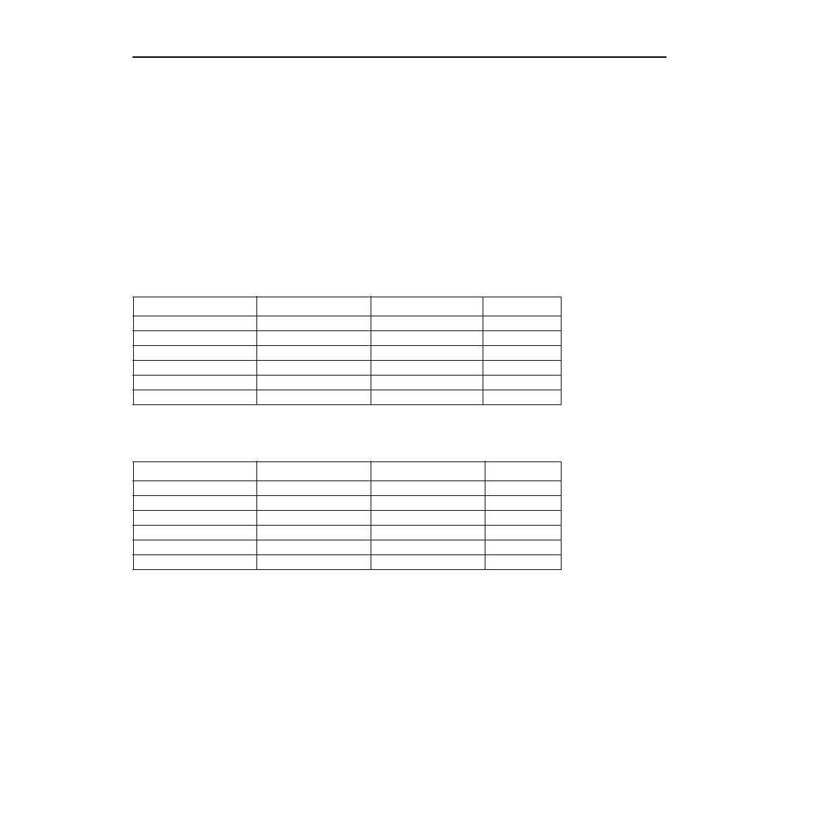
Table 4. Transmit PLL Clock and Data Rates
Note: The selection of full-rate or half-rate for a given reference clock speed is set by a bit in the transmit control register and can be set per
channel.
Table 5. Receive PLL Clock and Data Rates
Note: The selection of full-rate or half-rate for a given reference clock speed is set by a bit in the receive control register and can be set per
channel.
Reference Clock
There are two pairs of reference clock inputs on the ORT82G5. The differential reference clock is distributed to all
four channels in a quad. Each channel has a differential buffer to isolate the clock from the other channels. The
input clock is preferably a differential signal; however, the device can operate with a single-ended input. The input
reference clock directly impacts the transmit data eye, so the clock should have low jitter. In particular, jitter compo-
nents in the dc—5 MHz range should be minimized.
Note: The reference clock, REFCLK, is equivalent to REFINP and REFINN; throughout the text simply refer to the
reference clock as REFCLK.
For more information on the reference clock input requirements and connections to either single ended or differen-
tial inputs, see the SERDES reference clock application note.
Data Rate
Reference Clock
TCK78[A, B] Clock
Rate
1.0 Gbits/s
100 MHz
25 MHz
Half
1.25 Gbits/s
125 MHz
31.25 MHz
Half
2.0 Gbits/s
100 MHz
50 MHz
Full
2.5 Gbits/s
125 MHz
62.5 MHz
Full
3.125 Gbits/s
156 MHz
78 MHz
Full
3.5 Gbits/s
175 MHz
87.5 MHz
Full
Data Rate
Reference Clock
RWCKx Clocks
Rate
1.0 Gbits/s
100 MHz
25 MHz
Half
1.25 Gbits/s
125 MHz
31.25 MHz
Half
2.0 Gbits/s
100 MHz
50 MHz
Full
2.5 Gbits/s
125 MHz
62.5 MHz
Full
3.125 Gbits/s
156 MHz
78 MHz
Full
3.5 Gbits/s
175 MHz
87.5 MHz
Full
相關(guān)PDF資料 |
PDF描述 |
|---|---|
| ORT82G5-3BM680 | FPGA, 1296 CLBS, 380000 GATES, PBGA680 |
| OS10040280G-012 | FIBER OPTIC RECEIVER, 1290-1600nm, PANEL MOUNT, FC/APC CONNECTOR |
| OT-WBSC-Y-A-10-X-9-M-3-05-FA | FIBER OPTIC SPLITTER/COUPLER, 1X2PORT, 10.0, PANEL MOUNT, FC/APC CONNECTOR |
| OT-WBSC-Y-A-50-13-9-F-1-05-FA | FIBER OPTIC SPLITTER/COUPLER, 1X2PORT, 50.0, PANEL MOUNT, FC/APC CONNECTOR |
| OT-WBSC-Y-A-50-X-9-O-1-99-SA | FIBER OPTIC SPLITTER/COUPLER, 1X2PORT, 50.0, PANEL MOUNT, SC/APC CONNECTOR |
相關(guān)代理商/技術(shù)參數(shù) |
參數(shù)描述 |
|---|---|
| ORT82G5-2BM680C | 功能描述:FPGA - 現(xiàn)場可編程門陣列 10368 LUT 372 I/O RoHS:否 制造商:Altera Corporation 系列:Cyclone V E 柵極數(shù)量: 邏輯塊數(shù)量:943 內(nèi)嵌式塊RAM - EBR:1956 kbit 輸入/輸出端數(shù)量:128 最大工作頻率:800 MHz 工作電源電壓:1.1 V 最大工作溫度:+ 70 C 安裝風(fēng)格:SMD/SMT 封裝 / 箱體:FBGA-256 |
| ORT82G5-2BM680I | 功能描述:FPGA - 現(xiàn)場可編程門陣列 10368 LUT 372 I/O RoHS:否 制造商:Altera Corporation 系列:Cyclone V E 柵極數(shù)量: 邏輯塊數(shù)量:943 內(nèi)嵌式塊RAM - EBR:1956 kbit 輸入/輸出端數(shù)量:128 最大工作頻率:800 MHz 工作電源電壓:1.1 V 最大工作溫度:+ 70 C 安裝風(fēng)格:SMD/SMT 封裝 / 箱體:FBGA-256 |
| ORT82G5-2F680C | 功能描述:FPGA - 現(xiàn)場可編程門陣列 ORCA FPSC 2.7Gbits/s BP XCVR 643K RoHS:否 制造商:Altera Corporation 系列:Cyclone V E 柵極數(shù)量: 邏輯塊數(shù)量:943 內(nèi)嵌式塊RAM - EBR:1956 kbit 輸入/輸出端數(shù)量:128 最大工作頻率:800 MHz 工作電源電壓:1.1 V 最大工作溫度:+ 70 C 安裝風(fēng)格:SMD/SMT 封裝 / 箱體:FBGA-256 |
| ORT82G5-2F680I | 功能描述:FPGA - 現(xiàn)場可編程門陣列 ORCA FPSC 2.7GBITS/s BP XCVR 643K RoHS:否 制造商:Altera Corporation 系列:Cyclone V E 柵極數(shù)量: 邏輯塊數(shù)量:943 內(nèi)嵌式塊RAM - EBR:1956 kbit 輸入/輸出端數(shù)量:128 最大工作頻率:800 MHz 工作電源電壓:1.1 V 最大工作溫度:+ 70 C 安裝風(fēng)格:SMD/SMT 封裝 / 箱體:FBGA-256 |
| ORT82G5-2FN680C | 功能描述:FPGA - 現(xiàn)場可編程門陣列 ORCA FPSC 1.5V 3.7 G b Bpln Xcvr 643K Gt RoHS:否 制造商:Altera Corporation 系列:Cyclone V E 柵極數(shù)量: 邏輯塊數(shù)量:943 內(nèi)嵌式塊RAM - EBR:1956 kbit 輸入/輸出端數(shù)量:128 最大工作頻率:800 MHz 工作電源電壓:1.1 V 最大工作溫度:+ 70 C 安裝風(fēng)格:SMD/SMT 封裝 / 箱體:FBGA-256 |
發(fā)布緊急采購,3分鐘左右您將得到回復(fù)。