- 您現(xiàn)在的位置:買賣IC網(wǎng) > PDF目錄383714 > OR2T04A-4BA208 (Electronic Theatre Controls, Inc.) Field-Programmable Gate Arrays PDF資料下載
參數(shù)資料
| 型號: | OR2T04A-4BA208 |
| 廠商: | Electronic Theatre Controls, Inc. |
| 元件分類: | FPGA |
| 英文描述: | Field-Programmable Gate Arrays |
| 中文描述: | 現(xiàn)場可編程門陣列 |
| 文件頁數(shù): | 55/192頁 |
| 文件大?。?/td> | 3148K |
| 代理商: | OR2T04A-4BA208 |
第1頁第2頁第3頁第4頁第5頁第6頁第7頁第8頁第9頁第10頁第11頁第12頁第13頁第14頁第15頁第16頁第17頁第18頁第19頁第20頁第21頁第22頁第23頁第24頁第25頁第26頁第27頁第28頁第29頁第30頁第31頁第32頁第33頁第34頁第35頁第36頁第37頁第38頁第39頁第40頁第41頁第42頁第43頁第44頁第45頁第46頁第47頁第48頁第49頁第50頁第51頁第52頁第53頁第54頁當前第55頁第56頁第57頁第58頁第59頁第60頁第61頁第62頁第63頁第64頁第65頁第66頁第67頁第68頁第69頁第70頁第71頁第72頁第73頁第74頁第75頁第76頁第77頁第78頁第79頁第80頁第81頁第82頁第83頁第84頁第85頁第86頁第87頁第88頁第89頁第90頁第91頁第92頁第93頁第94頁第95頁第96頁第97頁第98頁第99頁第100頁第101頁第102頁第103頁第104頁第105頁第106頁第107頁第108頁第109頁第110頁第111頁第112頁第113頁第114頁第115頁第116頁第117頁第118頁第119頁第120頁第121頁第122頁第123頁第124頁第125頁第126頁第127頁第128頁第129頁第130頁第131頁第132頁第133頁第134頁第135頁第136頁第137頁第138頁第139頁第140頁第141頁第142頁第143頁第144頁第145頁第146頁第147頁第148頁第149頁第150頁第151頁第152頁第153頁第154頁第155頁第156頁第157頁第158頁第159頁第160頁第161頁第162頁第163頁第164頁第165頁第166頁第167頁第168頁第169頁第170頁第171頁第172頁第173頁第174頁第175頁第176頁第177頁第178頁第179頁第180頁第181頁第182頁第183頁第184頁第185頁第186頁第187頁第188頁第189頁第190頁第191頁第192頁
Data Sheet
June 1999
ORCA Series 2 FPGAs
Lucent Technologies Inc.
55
Special Function Blocks
(continued)
5-4488(F)
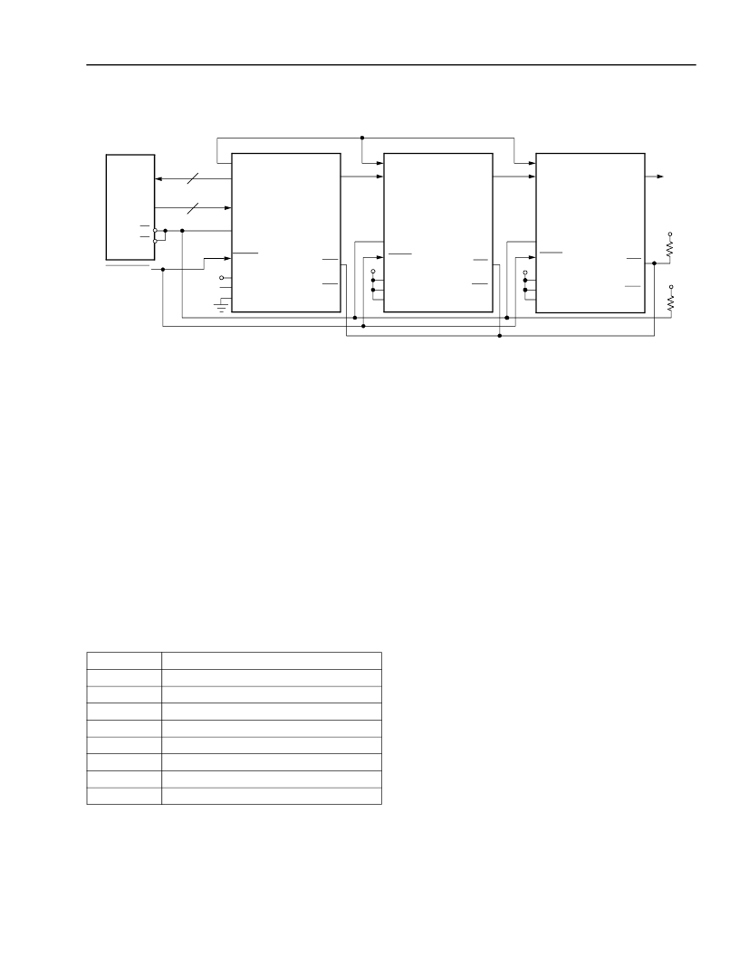
Figure 48. Boundary-Scan Interface
V
DD
EPROM
PROGRAM
D[7:0]
OE
CE
A[17:0]
A[17:0]
D[7:0]
DONE
M2
M1
M0
DONE
HDC
LDC
RCLK
CCLK
DIN
DOUT
DOUT
DIN
CCLK
DONE
DOUT
INIT
INIT
INIT
CCLK
V
V
DD
OR
GND
PRGM
PRGM
M2
M1
M0
PRGM
M2
M1
M0
V
DD
V
DD
HDC
LDC
RCLK
HDC
LDC
RCLK
V
DD
ORCA
SERIES
FPGA
SLAVE #2
ORCA
SERIES
FPGA
MASTER
ORCA
SERIES
FPGA
SLAVE #1
The BSM also increases test throughput with a dedi-
cated automatic test-pattern generator and with com-
pression of the test response with a signature analysis
register. The PC-based boundary-scan test card/soft-
ware allows a user to quickly prototype a boundary-
scan test setup.
Boundary-Scan Instructions
The ORCA Series boundary-scan circuitry is used for
three mandatory IEEE1149.1 tests (EXTEST, SAM-
PLE/PRELOAD, BYPASS) and four ORCA-defined
instructions. The 3-bit wide instruction register sup-
ports the eight instructions listed in Table 12.
Table 12. Boundary-Scan Instructions
The external test (EXTEST) instruction allows the inter-
connections between ICs in a system to be tested for
opens and stuck-at faults. If an EXTEST instruction is
performed for the system shown in Figure 47, the con-
nections between U1 and U2 (shown by nets a, b, and
c) can be tested by driving a value onto the given nets
from one device and then determining whether the
same value is seen at the other device. This is deter-
mined by shifting 2 bits of data for each pin (one for the
output value and one for the 3-state value) through the
BSR until each one aligns to the appropriate pin.
Then, based upon the value of the 3-state signal, either
the I/O pad is driven to the value given in the BSR, or
the BSR is updated with the input value from the I/O
pad, which allows it to be shifted out TDO.
The SAMPLE instruction is useful for system debug-
ging and fault diagnosis by allowing the data at the
FPGA’s I/Os to be observed during normal operation.
The data for all of the I/Os is captured simultaneously
into the BSR, allowing them to be shifted-out TDO to
the test host. Since each I/O buffer in the PICs is bidi-
rectional, two pieces of data are captured for each I/O
pad: the value at the I/O pad and the value of the
3-state control signal.
Code
000
001
010
011
100
101
110
111
Instruction
EXTEST
PLC Scan Ring 1
RAM Write (RAM_W)
Reserved
SAMPLE/PRELOAD
PLC Scan Ring 2
RAM Read (RAM_R)
BYPASS
相關PDF資料 |
PDF描述 |
|---|---|
| OR2T04A-4BA208I | Field-Programmable Gate Arrays |
| OR2T04A-4BA84 | Field-Programmable Gate Arrays |
| OR2T04A-4BA84I | Field-Programmable Gate Arrays |
| OR2T04A-4BC100 | Field-Programmable Gate Arrays |
| OR2T04A-4BC100I | Field-Programmable Gate Arrays |
相關代理商/技術參數(shù) |
參數(shù)描述 |
|---|---|
| OR2T04A-4BA208I | 制造商:未知廠家 制造商全稱:未知廠家 功能描述:Field-Programmable Gate Arrays |
| OR2T04A-4BA84 | 制造商:未知廠家 制造商全稱:未知廠家 功能描述:Field-Programmable Gate Arrays |
| OR2T04A-4BA84I | 制造商:未知廠家 制造商全稱:未知廠家 功能描述:Field-Programmable Gate Arrays |
| OR2T04A-4BC100 | 制造商:未知廠家 制造商全稱:未知廠家 功能描述:Field-Programmable Gate Arrays |
| OR2T04A-4BC100I | 制造商:未知廠家 制造商全稱:未知廠家 功能描述:Field-Programmable Gate Arrays |
發(fā)布緊急采購,3分鐘左右您將得到回復。