- 您現(xiàn)在的位置:買賣IC網(wǎng) > PDF目錄98045 > MTB40N10E (ON SEMICONDUCTOR) 40 A, 100 V, 0.04 ohm, N-CHANNEL, Si, POWER, MOSFET PDF資料下載
參數(shù)資料
| 型號(hào): | MTB40N10E |
| 廠商: | ON SEMICONDUCTOR |
| 元件分類: | JFETs |
| 英文描述: | 40 A, 100 V, 0.04 ohm, N-CHANNEL, Si, POWER, MOSFET |
| 封裝: | D2PAK-3 |
| 文件頁(yè)數(shù): | 1/12頁(yè) |
| 文件大?。?/td> | 119K |
| 代理商: | MTB40N10E |
Semiconductor Components Industries, LLC, 2000
November, 2000 – Rev. 2
1
Publication Order Number:
MTB40N10E/D
MTB40N10E
Preferred Device
Power MOSFET
40 Amps, 100 Volts
N–Channel D2PAK
This Power MOSFET is designed to withstand high energy in the
avalanche and commutation modes. The energy efficient design also
offers a drain–to–source diode with a fast recovery time. Designed for
low voltage, high speed switching applications in power supplies,
converters and PWM motor controls, these devices are particularly
well suited for bridge circuits where diode speed and commutating
safe operating areas are critical and offer additional safety margin
against unexpected voltage transients.
Avalanche Energy Specified
Source–to–Drain Diode Recovery Time Comparable to a
Discrete Fast Recovery Diode
Diode is Characterized for Use in Bridge Circuits
IDSS and VDS(on) Specified at Elevated Temperature
MAXIMUM RATINGS (TC = 25°C unless otherwise noted)
Rating
Symbol
Value
Unit
Drain–to–Source Voltage
VDSS
100
Vdc
Drain–to–Gate Voltage (RGS = 1.0 M)
VDGR
100
Vdc
Gate–to–Source Voltage
– Continuous
– Non–Repetitive (tp ≤ 10 ms)
VGS
VGSM
± 20
± 40
Vdc
Vpk
Drain Current – Continuous
Drain Current – Continuous @ 100
°C
Drain Current – Single Pulse (tp ≤ 10 s)
ID
IDM
40
29
140
Adc
Apk
Total Power Dissipation
Derate above 25
°C
Total Power Dissipation @ TA = 25°C
(Note 1.)
PD
169
1.35
2.5
Watts
W/
°C
Watts
Operating and Storage Temperature
Range
TJ, Tstg
– 55 to
150
°C
Single Pulse Drain–to–Source Avalanche
Energy – Starting TJ = 25°C
(VDD = 75 Vdc, VGS = 10 Vdc, Peak
IL = 40 Apk, L = 1.0 mH, RG = 25 )
EAS
800
mJ
Thermal Resistance
– Junction to Case
– Junction to Ambient
– Junction to Ambient (Note 1.)
R
θJC
R
θJA
R
θJA
0.74
62.5
50
°C/W
Maximum Lead Temperature for Soldering
Purposes, 1/8
″ from case for 10
seconds
TL
260
°C
1. When surface mounted to an FR4 board using the minimum recommended
pad size.
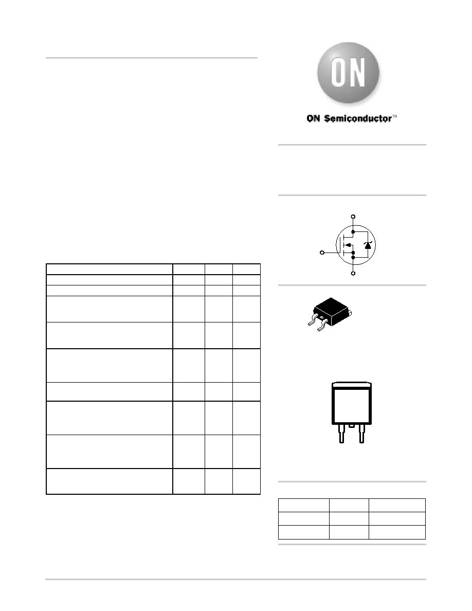
MARKING DIAGRAM
& PIN ASSIGNMENT
T40N10E
YWW
1
Gate
4
Drain
2
Drain
3
Source
40 AMPERES
100 VOLTS
RDS(on) = 40 m
Device
Package
Shipping
ORDERING INFORMATION
MTB40N10E
D2PAK
50 Units/Rail
D2PAK
CASE 418B
STYLE 2
1
2
3
4
http://onsemi.com
N–Channel
D
S
G
T40N10E
= Device Code
Y
= Year
WW
= Work Week
MTB40N10ET4
D2PAK
800/Tape & Reel
Preferred devices are recommended choices for future use
and best overall value.
相關(guān)PDF資料 |
PDF描述 |
|---|---|
| MTB40N10ET4 | 40 A, 100 V, 0.04 ohm, N-CHANNEL, Si, POWER, MOSFET |
| MTB50N06VLT4 | 42 A, 60 V, 0.032 ohm, N-CHANNEL, Si, POWER, MOSFET |
| MTB50N06VL | 42 A, 60 V, 0.032 ohm, N-CHANNEL, Si, POWER, MOSFET |
| MTB50P03HDLT4 | 50 A, 30 V, 0.03 ohm, P-CHANNEL, Si, POWER, MOSFET |
| MTB52N06VLT4 | 52 A, 60 V, 0.025 ohm, N-CHANNEL, Si, POWER, MOSFET |
相關(guān)代理商/技術(shù)參數(shù) |
參數(shù)描述 |
|---|---|
| MTB40N10ET4 | 制造商:ON Semiconductor 功能描述:Trans MOSFET N-CH 100V 40A 3-Pin(2+Tab) D2PAK T/R |
| MTB44P04J3 | 制造商:CYSTEKEC 制造商全稱:Cystech Electonics Corp. 功能描述:P-Channel Enhancement Mode Power MOSFET |
| MTB45A06Q8 | 制造商:CYSTEKEC 制造商全稱:Cystech Electonics Corp. 功能描述:Dual N-Channel Logic Level Enhancement Mode Power MOSFET |
| MTB4N40ET4 | 制造商:Rochester Electronics LLC 功能描述:- Bulk |
| MTB4N50ET4 | 制造商:Rochester Electronics LLC 功能描述:- Bulk 制造商:ON Semiconductor 功能描述: |
發(fā)布緊急采購(gòu),3分鐘左右您將得到回復(fù)。