- 您現(xiàn)在的位置:買賣IC網(wǎng) > PDF目錄98023 > MM908E621ACDWB/R2 (FREESCALE SEMICONDUCTOR INC) 8-BIT, FLASH, 8 MHz, MICROCONTROLLER, PDSO54 PDF資料下載
參數(shù)資料
| 型號: | MM908E621ACDWB/R2 |
| 廠商: | FREESCALE SEMICONDUCTOR INC |
| 元件分類: | 微控制器/微處理器 |
| 英文描述: | 8-BIT, FLASH, 8 MHz, MICROCONTROLLER, PDSO54 |
| 封裝: | 17.90 X 7.50 MM, 0.65 MM PITCH, PLASTIC, SOIC-54 |
| 文件頁數(shù): | 27/65頁 |
| 文件大小: | 1221K |
| 代理商: | MM908E621ACDWB/R2 |
第1頁第2頁第3頁第4頁第5頁第6頁第7頁第8頁第9頁第10頁第11頁第12頁第13頁第14頁第15頁第16頁第17頁第18頁第19頁第20頁第21頁第22頁第23頁第24頁第25頁第26頁當前第27頁第28頁第29頁第30頁第31頁第32頁第33頁第34頁第35頁第36頁第37頁第38頁第39頁第40頁第41頁第42頁第43頁第44頁第45頁第46頁第47頁第48頁第49頁第50頁第51頁第52頁第53頁第54頁第55頁第56頁第57頁第58頁第59頁第60頁第61頁第62頁第63頁第64頁第65頁
Analog Integrated Circuit Device Data
Freescale Semiconductor
33
908E621
FUNCTIONAL DEVICE OPERATION
OPERATIONAL MODES
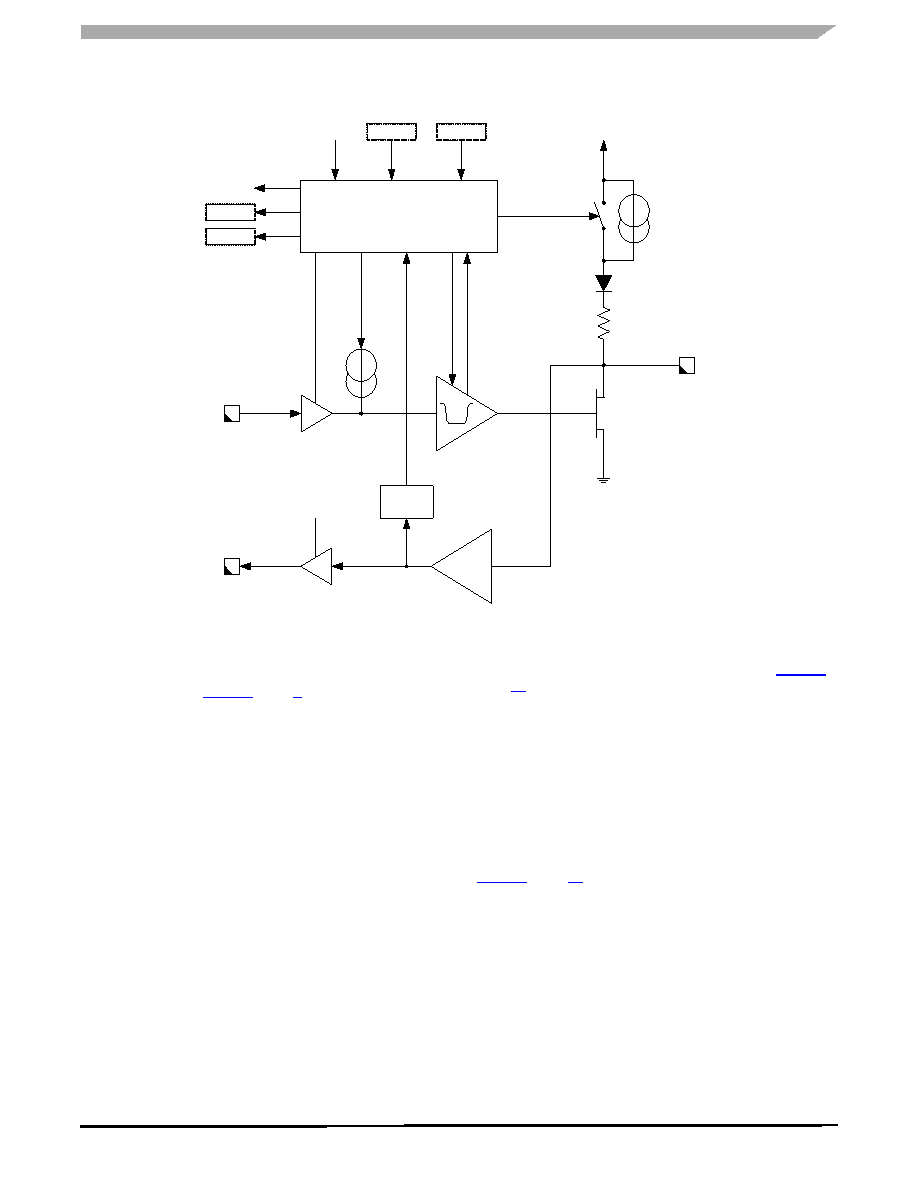
Figure 16. LIN Interface
TXD Pin
The TXD pin is the MCU interface to control the state of the
LIN transmitter (see Figure 2, page 2). When TXD is LOW,
the LIN pin is low (dominant state). When TXD is HIGH, the
LIN output MOSFET is turned off (recessive state). The TXD
pin has an internal pull-up current source to set the LIN bus
to a recessive state in the event, for instance, if the
microcontroller could not control it during system power-up or
power-down.
RXD Pin
The RXD transceiver pin is the MCU interface, which
reports the state of the LIN bus voltage. LIN HIGH (recessive
state) is reported by a high level on RXD, LIN LOW (dominant
state) by a low level on RXD.
STOP Mode and Wake-up Feature
During STOP mode operation the transmitter of the
physical layer is disabled and the internal pullup resistor is
disconnected from VSUP and a small current source keeps
the LIN pin in recessive state. The receiver is still active and
able to detect wake-up events on the LIN bus line.
If the LIN interrupt is enabled (LINIE bit in the Interrupt
Mask register is set), a dominant level longer than TPROPWL
followed by an rising edge will set the LINIF flag and generate
an interrupt which causes a system wake-up (see Figure 8,
SLEEP Mode and Wake-up Feature
During SLEEP mode operation the transmitter of the
physical layer is disabled, the internal pullup resistor is
disconnected from VSUP, and a small current source keeps
the LIN pin in the recessive state. The receiver is still active
to be able to detect wake-up events on the LIN bus line.
A dominant level longer than TPROPWL followed by an
rising edge will generate a system wake-up (reset) and set
the LINWF flag in the Reset Status register (RSR). Also see
A0 INPUT AND ANALOG MULTIPLEXER
A0 - Analog Input
Input A0 is an analog input used for reading switches, or
as analog inputs for potentiometers, NTC, etc.
A0 is internally connected to the analog multiplexer. This
pin offers a switchable current source. To read the Analog
Input, the pin has to be selected with the SS[3:0] bits in the
A0MUCTL register.
Control
Receiv
er
Wake-up
RXD
TXD
GND
VSUP
Slope
Control
30k
10A
LIN bus
SRS[1:0]
PSON
LINCL
LINIF
Wake-up
Filter
MODE
TESTMODE
相關(guān)PDF資料 |
PDF描述 |
|---|---|
| MM908E621ACDWB | 8-BIT, FLASH, 8 MHz, MICROCONTROLLER, PDSO54 |
| MM908E622ACDWB/R2 | 8-BIT, FLASH, 8 MHz, MICROCONTROLLER, PDSO54 |
| MM908E624ACDWB/R | 8-BIT, FLASH, 8 MHz, MICROCONTROLLER, PDSO54 |
| MM908E625ACDWB | 8-BIT, FLASH, 8 MHz, MICROCONTROLLER, PDSO54 |
| MMBD1010LT3 | 0.2 A, 2 ELEMENT, SILICON, SIGNAL DIODE, TO-236AB |
相關(guān)代理商/技術(shù)參數(shù) |
參數(shù)描述 |
|---|---|
| MM908E621ACPEK | 功能描述:8位微控制器 -MCU QUAD H-B/3-HS W/MCU & LI RoHS:否 制造商:Silicon Labs 核心:8051 處理器系列:C8051F39x 數(shù)據(jù)總線寬度:8 bit 最大時鐘頻率:50 MHz 程序存儲器大小:16 KB 數(shù)據(jù) RAM 大小:1 KB 片上 ADC:Yes 工作電源電壓:1.8 V to 3.6 V 工作溫度范圍:- 40 C to + 105 C 封裝 / 箱體:QFN-20 安裝風格:SMD/SMT |
| MM908E621ACPEKR2 | 功能描述:8位微控制器 -MCU QUAD HB AND TRIPLE HS RoHS:否 制造商:Silicon Labs 核心:8051 處理器系列:C8051F39x 數(shù)據(jù)總線寬度:8 bit 最大時鐘頻率:50 MHz 程序存儲器大小:16 KB 數(shù)據(jù) RAM 大小:1 KB 片上 ADC:Yes 工作電源電壓:1.8 V to 3.6 V 工作溫度范圍:- 40 C to + 105 C 封裝 / 箱體:QFN-20 安裝風格:SMD/SMT |
| MM908E622 | 制造商:FREESCALE 制造商全稱:Freescale Semiconductor, Inc 功能描述:Integrated Quad Half-Bridge, Triple High-Side and EC Glass Driver with Embedded MCU and LIN for High End Mirror |
| MM908E622_08 | 制造商:FREESCALE 制造商全稱:Freescale Semiconductor, Inc 功能描述:Integrated Quad Half-bridge, Triple High Side and EC Glass Driver with Embedded MCU and LIN for High End Mirror |
| MM908E622ACDR2 | 制造商:FREESCALE 制造商全稱:Freescale Semiconductor, Inc 功能描述:Integrated Quad Half-Bridge, Triple High-Side and EC Glass Driver with Embedded MCU and LIN for High End Mirror |
發(fā)布緊急采購,3分鐘左右您將得到回復。