- 您現(xiàn)在的位置:買賣IC網(wǎng) > PDF目錄45312 > MCF5484CZP200 (MOTOROLA INC) 32-BIT, 200 MHz, RISC PROCESSOR, PBGA388 PDF資料下載
參數(shù)資料
| 型號: | MCF5484CZP200 |
| 廠商: | MOTOROLA INC |
| 元件分類: | 微控制器/微處理器 |
| 英文描述: | 32-BIT, 200 MHz, RISC PROCESSOR, PBGA388 |
| 封裝: | 27 X 27 MM, 1 MM PITCH, PLASTIC, MS-034AAL-1, BGA-388 |
| 文件頁數(shù): | 28/96頁 |
| 文件大小: | 2006K |
| 代理商: | MCF5484CZP200 |
第1頁第2頁第3頁第4頁第5頁第6頁第7頁第8頁第9頁第10頁第11頁第12頁第13頁第14頁第15頁第16頁第17頁第18頁第19頁第20頁第21頁第22頁第23頁第24頁第25頁第26頁第27頁當(dāng)前第28頁第29頁第30頁第31頁第32頁第33頁第34頁第35頁第36頁第37頁第38頁第39頁第40頁第41頁第42頁第43頁第44頁第45頁第46頁第47頁第48頁第49頁第50頁第51頁第52頁第53頁第54頁第55頁第56頁第57頁第58頁第59頁第60頁第61頁第62頁第63頁第64頁第65頁第66頁第67頁第68頁第69頁第70頁第71頁第72頁第73頁第74頁第75頁第76頁第77頁第78頁第79頁第80頁第81頁第82頁第83頁第84頁第85頁第86頁第87頁第88頁第89頁第90頁第91頁第92頁第93頁第94頁第95頁第96頁
34
MCF548x Integrated Microprocessor Hardware Specifications
MOTOROLA
PRELIMINARY—SUBJECT TO CHANGE WITHOUT NOTICE
Signal Description
1.5.1.5.1
Reset In (RSTI)
Asserting RSTI causes the MCF548x to enter reset exception processing. RSTO is asserted automatically
when RSTI is asserted.
1.5.1.5.2
Reset Out (RSTO)
After RSTI is asserted, the PLL temporarily loses its lock, during which time RSTO is asserted. When the
PLL regains its lock, RSTO negates again. This signal can be used to reset external devices.
1.5.1.5.3
Clock In (CLKIN)
CLKIN is the MCF548x input clock frequency to the on-board phase-locked loop (PLL) clock generator.
CLKIN is used to internally clock or sequence the MCF548x internal bus interface at a selected multiple of
the input frequency used for internal module logic. CLKIN is used as the clock reference for PCI and
FlexBus transfers.
1.5.1.6
Reset Configuration Pins
This section describes address/data pins, AD[12:0], that are read at reset to configure the MCF548x.
1.5.1.6.1
AD[12:8] / CLKIN to SDCLK Ratio (CLKCONFIG[4:0])
The clock configuration inputs, CLKCONFIG[4:0], indicate the CLKIN to SDCLK ratio. CLKIN is used
as the external reference for both PCI and FlexBus cycles. The CLKIN to SDCLK ratio is selectable, where
SDCLK is the clock frequency used for SDRAM accesses and the internal XLB bus. The core is always
clocked at twice the SDCLK frequency.
These signals are sampled on the rising edge of RSTI. Table 6 shows how the logic levels of AD[12:8]
correspond to the selected clock ratio.
1.5.1.6.2
AD5—FlexBus Size Configuration (FBSIZE)
At reset, the enabling and disabling of BE/BWE[3:0] versus TSIZ[1:0] and ADDR[1:0] is determined by
the logic level driven on AD5 at the rising edge of RSTI. FBSIZE is multiplexed with AD5 and sampled
only at reset. Table 7 shows how the AD5 logic level corresponds to the BE/BWE[3:0] function.
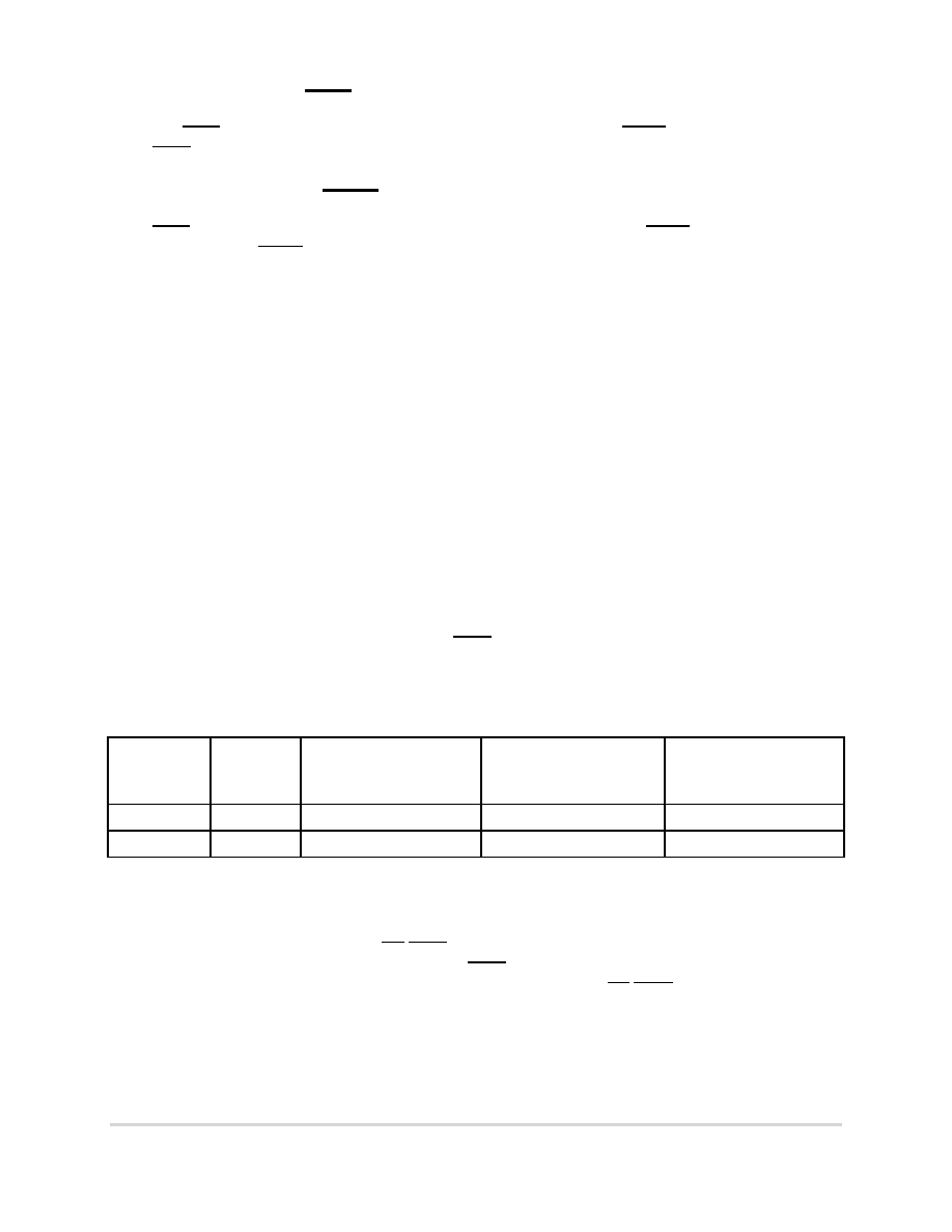
Table 6. MCF548X Divide Ratio Encodings
FB_AD[12:8]1
1
All other values of FB_AD[12:8] are reserved.
Clock Ratio
CLKIN—PCI and FlexBus
Frequency Range
(MHz)
Internal XLB and SDRAM
Bus Frequency Range
(MHz)
Core Frequency Range
(MHz)
00011
1:2
41.6–50.0
83.33–100
166.66–200
00101
1:2
30.0–44.4
60.0–88.8
120.0–177.66
相關(guān)PDF資料 |
PDF描述 |
|---|---|
| MCF5485CVR200 | 32-BIT, 200 MHz, RISC PROCESSOR, PBGA388 |
| MCF5483CVR166 | 32-BIT, 166.66 MHz, RISC PROCESSOR, PBGA388 |
| MCF5481CZP166 | 32-BIT, 166.66 MHz, RISC PROCESSOR, PBGA388 |
| MCF5484CVR200 | 32-BIT, 200 MHz, RISC PROCESSOR, PBGA388 |
| MCF5481CVR166 | 32-BIT, 166.66 MHz, RISC PROCESSOR, PBGA388 |
相關(guān)代理商/技術(shù)參數(shù) |
參數(shù)描述 |
|---|---|
| MCF5485 | 制造商:FREESCALE 制造商全稱:Freescale Semiconductor, Inc 功能描述:MCF548x ColdFire㈢ Microprocessor |
| MCF5485CVR200 | 功能描述:微處理器 - MPU MCF548X V4ECORE MMU FPU RoHS:否 制造商:Atmel 處理器系列:SAMA5D31 核心:ARM Cortex A5 數(shù)據(jù)總線寬度:32 bit 最大時(shí)鐘頻率:536 MHz 程序存儲(chǔ)器大小:32 KB 數(shù)據(jù) RAM 大小:128 KB 接口類型:CAN, Ethernet, LIN, SPI,TWI, UART, USB 工作電源電壓:1.8 V to 3.3 V 最大工作溫度:+ 85 C 安裝風(fēng)格:SMD/SMT 封裝 / 箱體:FBGA-324 |
| MCF5485CZP200 | 功能描述:微處理器 - MPU MCF548X V4ECORE MMU FPU RoHS:否 制造商:Atmel 處理器系列:SAMA5D31 核心:ARM Cortex A5 數(shù)據(jù)總線寬度:32 bit 最大時(shí)鐘頻率:536 MHz 程序存儲(chǔ)器大小:32 KB 數(shù)據(jù) RAM 大小:128 KB 接口類型:CAN, Ethernet, LIN, SPI,TWI, UART, USB 工作電源電壓:1.8 V to 3.3 V 最大工作溫度:+ 85 C 安裝風(fēng)格:SMD/SMT 封裝 / 箱體:FBGA-324 |
| MCF548X | 制造商:FREESCALE 制造商全稱:Freescale Semiconductor, Inc 功能描述:MCF548x ColdFire㈢ Microprocessor |
| MCF548X_07 | 制造商:FREESCALE 制造商全稱:Freescale Semiconductor, Inc 功能描述:MCF548x ColdFire㈢ Microprocessor |
發(fā)布緊急采購,3分鐘左右您將得到回復(fù)。