- 您現(xiàn)在的位置:買賣IC網(wǎng) > PDF目錄45211 > MC68307FG16 (MOTOROLA INC) 16-BIT, 16.67 MHz, MICROCONTROLLER, PQFP100 PDF資料下載
參數(shù)資料
| 型號(hào): | MC68307FG16 |
| 廠商: | MOTOROLA INC |
| 元件分類: | 微控制器/微處理器 |
| 英文描述: | 16-BIT, 16.67 MHz, MICROCONTROLLER, PQFP100 |
| 封裝: | PLASTIC, QFP-100 |
| 文件頁(yè)數(shù): | 19/264頁(yè) |
| 文件大?。?/td> | 949K |
| 代理商: | MC68307FG16 |
第1頁(yè)第2頁(yè)第3頁(yè)第4頁(yè)第5頁(yè)第6頁(yè)第7頁(yè)第8頁(yè)第9頁(yè)第10頁(yè)第11頁(yè)第12頁(yè)第13頁(yè)第14頁(yè)第15頁(yè)第16頁(yè)第17頁(yè)第18頁(yè)當(dāng)前第19頁(yè)第20頁(yè)第21頁(yè)第22頁(yè)第23頁(yè)第24頁(yè)第25頁(yè)第26頁(yè)第27頁(yè)第28頁(yè)第29頁(yè)第30頁(yè)第31頁(yè)第32頁(yè)第33頁(yè)第34頁(yè)第35頁(yè)第36頁(yè)第37頁(yè)第38頁(yè)第39頁(yè)第40頁(yè)第41頁(yè)第42頁(yè)第43頁(yè)第44頁(yè)第45頁(yè)第46頁(yè)第47頁(yè)第48頁(yè)第49頁(yè)第50頁(yè)第51頁(yè)第52頁(yè)第53頁(yè)第54頁(yè)第55頁(yè)第56頁(yè)第57頁(yè)第58頁(yè)第59頁(yè)第60頁(yè)第61頁(yè)第62頁(yè)第63頁(yè)第64頁(yè)第65頁(yè)第66頁(yè)第67頁(yè)第68頁(yè)第69頁(yè)第70頁(yè)第71頁(yè)第72頁(yè)第73頁(yè)第74頁(yè)第75頁(yè)第76頁(yè)第77頁(yè)第78頁(yè)第79頁(yè)第80頁(yè)第81頁(yè)第82頁(yè)第83頁(yè)第84頁(yè)第85頁(yè)第86頁(yè)第87頁(yè)第88頁(yè)第89頁(yè)第90頁(yè)第91頁(yè)第92頁(yè)第93頁(yè)第94頁(yè)第95頁(yè)第96頁(yè)第97頁(yè)第98頁(yè)第99頁(yè)第100頁(yè)第101頁(yè)第102頁(yè)第103頁(yè)第104頁(yè)第105頁(yè)第106頁(yè)第107頁(yè)第108頁(yè)第109頁(yè)第110頁(yè)第111頁(yè)第112頁(yè)第113頁(yè)第114頁(yè)第115頁(yè)第116頁(yè)第117頁(yè)第118頁(yè)第119頁(yè)第120頁(yè)第121頁(yè)第122頁(yè)第123頁(yè)第124頁(yè)第125頁(yè)第126頁(yè)第127頁(yè)第128頁(yè)第129頁(yè)第130頁(yè)第131頁(yè)第132頁(yè)第133頁(yè)第134頁(yè)第135頁(yè)第136頁(yè)第137頁(yè)第138頁(yè)第139頁(yè)第140頁(yè)第141頁(yè)第142頁(yè)第143頁(yè)第144頁(yè)第145頁(yè)第146頁(yè)第147頁(yè)第148頁(yè)第149頁(yè)第150頁(yè)第151頁(yè)第152頁(yè)第153頁(yè)第154頁(yè)第155頁(yè)第156頁(yè)第157頁(yè)第158頁(yè)第159頁(yè)第160頁(yè)第161頁(yè)第162頁(yè)第163頁(yè)第164頁(yè)第165頁(yè)第166頁(yè)第167頁(yè)第168頁(yè)第169頁(yè)第170頁(yè)第171頁(yè)第172頁(yè)第173頁(yè)第174頁(yè)第175頁(yè)第176頁(yè)第177頁(yè)第178頁(yè)第179頁(yè)第180頁(yè)第181頁(yè)第182頁(yè)第183頁(yè)第184頁(yè)第185頁(yè)第186頁(yè)第187頁(yè)第188頁(yè)第189頁(yè)第190頁(yè)第191頁(yè)第192頁(yè)第193頁(yè)第194頁(yè)第195頁(yè)第196頁(yè)第197頁(yè)第198頁(yè)第199頁(yè)第200頁(yè)第201頁(yè)第202頁(yè)第203頁(yè)第204頁(yè)第205頁(yè)第206頁(yè)第207頁(yè)第208頁(yè)第209頁(yè)第210頁(yè)第211頁(yè)第212頁(yè)第213頁(yè)第214頁(yè)第215頁(yè)第216頁(yè)第217頁(yè)第218頁(yè)第219頁(yè)第220頁(yè)第221頁(yè)第222頁(yè)第223頁(yè)第224頁(yè)第225頁(yè)第226頁(yè)第227頁(yè)第228頁(yè)第229頁(yè)第230頁(yè)第231頁(yè)第232頁(yè)第233頁(yè)第234頁(yè)第235頁(yè)第236頁(yè)第237頁(yè)第238頁(yè)第239頁(yè)第240頁(yè)第241頁(yè)第242頁(yè)第243頁(yè)第244頁(yè)第245頁(yè)第246頁(yè)第247頁(yè)第248頁(yè)第249頁(yè)第250頁(yè)第251頁(yè)第252頁(yè)第253頁(yè)第254頁(yè)第255頁(yè)第256頁(yè)第257頁(yè)第258頁(yè)第259頁(yè)第260頁(yè)第261頁(yè)第262頁(yè)第263頁(yè)第264頁(yè)
System Integration Module
5-20
MC68307 USER’S MANUAL
MOTOROLA
In the case of the UART, its clock is restarted automatically by a transition on the RxD pin,
so that incoming data is clocked in. When the data has been completely received, then an
interrupt from the UART can wake-up the core processor as described above. If the other
on-chip modules are required to cause a wake-up (the timer and M-bus), then their clocks
should not be gated off in this manner.
5.2 PROGRAMMING MODEL
The various modules in the MC68307, including the SIM, contain registers which are used
to control the modules and provide status information from the modules. Most of these
registers reside in one 4096-byte range of addresses in the memory map of the EC000 core
processor. The only exceptions to this rule are the MBAR and the SCR. These reside in the
initial memory map of the MC68307 overlaying Motorola-reserved locations of the exception
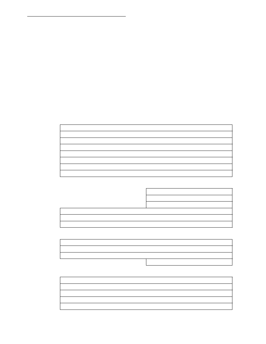
vector table. Table 5-5 shows all MC68307 on-chip locations.
Table 5-5. MC68307 Configuration Memory Map
Address
System Configuration Registers
$0000F0
Reserved–No External Bus Access
$0000F2
Module Base Address Register (MBAR)
$0000F4
System Control Register (SCR)
$0000F6
System Control Register (SCR), continued
$0000F8
Reserved–No External Bus Access
$000FA
Reserved–No External Bus Access
$0000FC
Reserved–No External Bus Access
$0000FE
Reserved–No External Bus Access
Address
SIM Module–External Bus Interface Registers
MBASE+$011
Do Not Access Byte $010
Port A Control Register (PACNT)
MBASE+$013
Do Not Access Byte $012
Port A Data Direction Register (PADDR)
MBASE+$015
Do Not Access Byte $014
Port A Data Register (PADAT)
MBASE+$016
Port B Control Register (PBCNT)
MBASE+$018
Port B Data Direction Register (PBDDR)
MBASE+$01A
Port B Data Register (PBDAT)
Address
SIM Module–Interrupt Controller Registers
MBASE+$020
Latched Interrupt Control Register 1 (LICR1)
MBASE+$022
Latched Interrupt Control Register 2 (LICR2)
MBASE+$024
Peripheral Interrupt Control Register (PICR)
MBASE+$027
Do Not Access Byte $026
Programmable Interrupt Vector Reg (PIVR)
Address
SIM Module–Chip Select Registers
MBASE+$040
Base Register 0 (BR0)
MBASE+$042
Option Register 0 (OR0)
MBASE+$044
Base Register 1 (BR1)
MBASE+$046
Option Register 1 (OR1)
MBASE+$048
Base Register 2 (BR2)
相關(guān)PDF資料 |
PDF描述 |
|---|---|
| MC68322FT16 | 16-BIT, 16.667 MHz, RISC PROCESSOR, PQFP160 |
| MC68331CFC20B1 | 32-BIT, 20 MHz, MICROCONTROLLER, PQFP132 |
| MC68331CPV20B1 | 32-BIT, 20 MHz, MICROCONTROLLER, PQFP144 |
| MC68331CFC25B1 | 32-BIT, 25 MHz, MICROCONTROLLER, PQFP132 |
| MC68331CPV16B1 | 32-BIT, 16 MHz, MICROCONTROLLER, PQFP144 |
相關(guān)代理商/技術(shù)參數(shù) |
參數(shù)描述 |
|---|---|
| MC68307UM | 制造商:MOTOROLA 制造商全稱:Motorola, Inc 功能描述:Technical Summary Integrated Multiple-Bus Processor |
| MC68307V | 制造商:MOTOROLA 制造商全稱:Motorola, Inc 功能描述:Technical Summary Integrated Multiple-Bus Processor |
| MC68322 | 制造商:MOTOROLA 制造商全稱:Motorola, Inc 功能描述:Integrated Printer Processor |
| MC68322AD | 制造商:MOTOROLA 制造商全稱:Motorola, Inc 功能描述:Integrated Printer Processor |
| MC68322FT20 | 制造商:Rochester Electronics LLC 功能描述:- Bulk |
發(fā)布緊急采購(gòu),3分鐘左右您將得到回復(fù)。