- 您現(xiàn)在的位置:買賣IC網(wǎng) > PDF目錄16982 > MAXADCLITE+ (Maxim Integrated Products)KIT EVALUATION FOR MAX11645 PDF資料下載
參數(shù)資料
| 型號: | MAXADCLITE+ |
| 廠商: | Maxim Integrated Products |
| 文件頁數(shù): | 6/22頁 |
| 文件大?。?/td> | 0K |
| 描述: | KIT EVALUATION FOR MAX11645 |
| 產(chǎn)品培訓(xùn)模塊: | Lead (SnPb) Finish for COTS Obsolescence Mitigation Program |
| 標(biāo)準(zhǔn)包裝: | 1 |
| ADC 的數(shù)量: | 1 |
| 位數(shù): | 12 |
| 采樣率(每秒): | 94.4k |
| 數(shù)據(jù)接口: | USB |
| 輸入范圍: | ±VREF/2 |
| 工作溫度: | -40°C ~ 85°C |
| 已用 IC / 零件: | MAX11645 |
| 已供物品: | 板,軟件 |
MAX11644/MAX11645
Low-Power, 1-/2-Channel, I2C, 12-Bit ADCs
in Ultra-Tiny 1.9mm x 2.2mm Package
14
______________________________________________________________________________________
Configuration/Setup Bytes (Write Cycle)
A write cycle begins with the bus master issuing a
START condition followed by seven address bits
(Figure 7) and a write bit (R/W = 0). If the address byte
is successfully received, the MAX11644/MAX11645
(slave) issues an acknowledge. The master then writes
to the slave. The slave recognizes the received byte as
the set-up byte (Table 1) if the most significant bit
(MSB) is 1. If the MSB is 0, the slave recognizes that
byte as the configuration byte (Table 2). The master
can write either one or two bytes to the slave in any
order (setup byte, then configuration byte; configura-
tion byte, then setup byte; setup byte or configuration
byte only; Figure 9). If the slave receives a byte suc-
cessfully, it issues an acknowledge. The master ends
the write cycle by issuing a STOP condition or a repeat-
ed START condition. When operating in HS mode, a
STOP condition returns the bus into F/S mode (see the
HS Mode section).
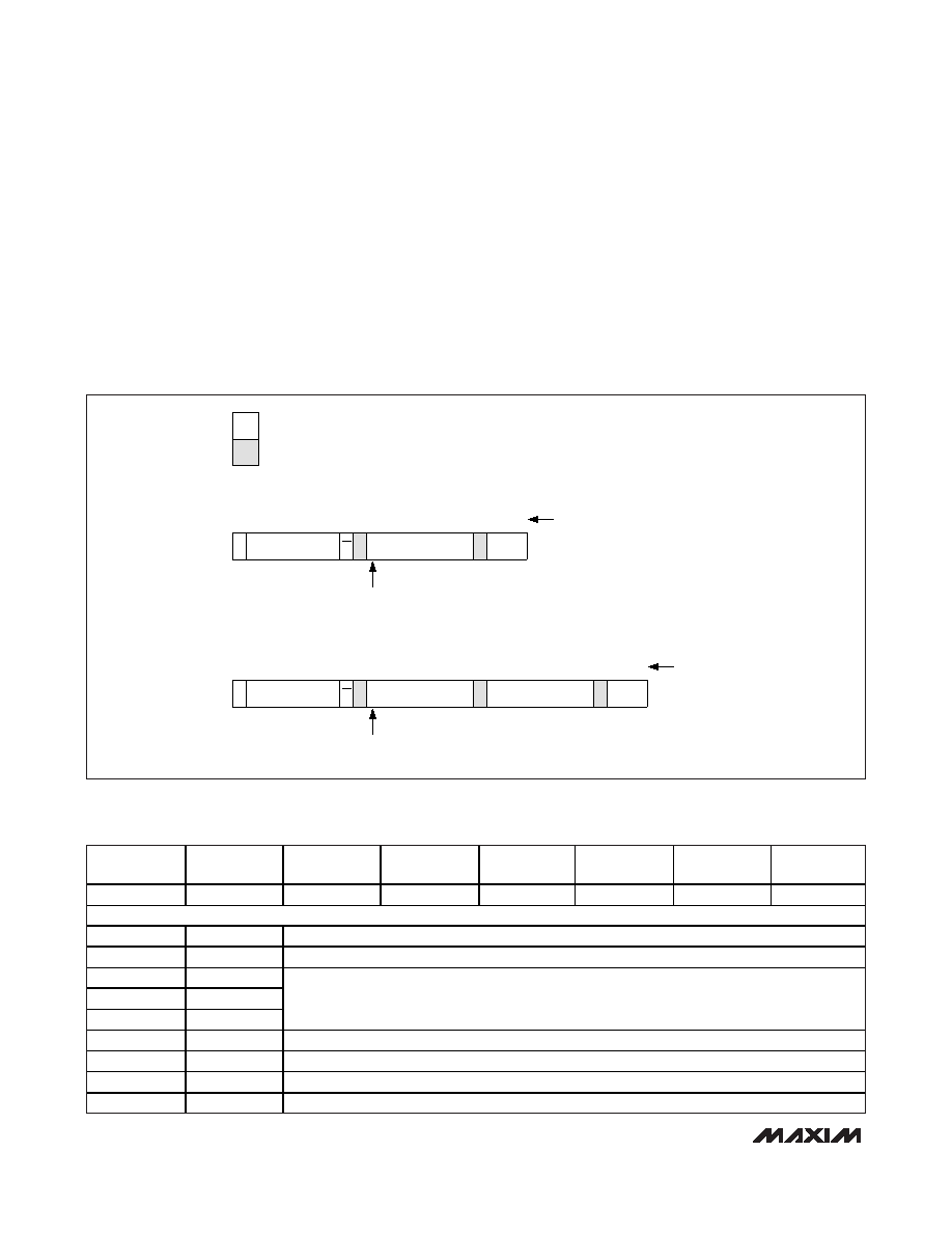
B) TWO-BYTE WRITE CYCLE
SLAVE TO MASTER
MASTER TO SLAVE
S
1
SLAVE ADDRESS
A
71 1
W
SETUP OR
CONFIGURATION BYTE
SETUP OR
CONFIGURATION BYTE
8
P OR Sr
1
A
1
MSB DETERMINES WHETHER
SETUP OR CONFIGURATION BYTE
S
1
SLAVE ADDRESS
A
71 1
W
SETUP OR
CONFIGURATION BYTE
8
P OR Sr
1
A
1
MSB DETERMINES WHETHER
SETUP OR CONFIGURATION BYTE
A
1
8
A) ONE-BYTE WRITE CYCLE
NUMBER OF BITS
Figure 9. Write Cycle
BIT 7
(MSB)
BIT 6
BIT 5
BIT 4
BIT 3
BIT 2
BIT 1
BIT 0
(LSB)
REG
SEL2
SEL1
SEL0
CLK
BIP/UNI
RST
X
BIT
NAME
DESCRIPTION
7
REG
Register bit. 1 = setup byte, 0 = configuration byte (Table 2).
6
SEL2
5
SEL1
4
SEL0
Three bits select the reference voltage (Table 6).
Default to 000 at power-up.
3
CLK
1 = external clock, 0 = internal clock. Defaults to 0 at power-up.
2
BIP/UNI
1 = bipolar, 0 = unipolar. Defaults to 0 at power-up (see the Unipolar/Bipolar section).
1
RST
1 = no action, 0 = resets the configuration register to default. Setup register remains unchanged.
0
X
Don’t-care bit. This bit can be set to 1 or 0.
Table 1. Setup Byte Format
相關(guān)PDF資料 |
PDF描述 |
|---|---|
| ESM08DTAN | CONN EDGECARD 16POS R/A .156 SLD |
| EMM08DTAN | CONN EDGECARD 16POS R/A .156 SLD |
| AD780BR-REEL | IC VREF SERIES SHUNT PREC 8-SOIC |
| LAR2E681MELB30 | CAP ALUM 680UF 250V 20% SNAP |
| ELL-6PV680M | COIL PWR CHOKE 68UH 420MA SMD |
相關(guān)代理商/技術(shù)參數(shù) |
參數(shù)描述 |
|---|---|
| MAXADCLITE# | 功能描述:數(shù)據(jù)轉(zhuǎn)換 IC 開發(fā)工具 MAX11645 Eval Kit RoHS:否 制造商:Texas Instruments 產(chǎn)品:Demonstration Kits 類型:ADC 工具用于評估:ADS130E08 接口類型:SPI 工作電源電壓:- 6 V to + 6 V |
| MAXADCLITE+ | 功能描述:數(shù)據(jù)轉(zhuǎn)換 IC 開發(fā)工具 MAX11645 Eval Kit RoHS:否 制造商:Texas Instruments 產(chǎn)品:Demonstration Kits 類型:ADC 工具用于評估:ADS130E08 接口類型:SPI 工作電源電壓:- 6 V to + 6 V |
| MAX-B550 | 制造商:SAMSUNG 制造商全稱:Samsung semiconductor 功能描述:THREE-CD CHANGER MINI-COMPACT SYSTEM CD-R/RW PLAYBACK |
| MAX-B570 | 制造商:SAMSUNG 制造商全稱:Samsung semiconductor 功能描述:THREE-CD CHANGER MINI-COMPACT SYSTEM CD-R/RW PLAYBACK |
| MAXC001 | 制造商:Maxim Integrated Products 功能描述: |
發(fā)布緊急采購,3分鐘左右您將得到回復(fù)。