- 您現(xiàn)在的位置:買賣IC網(wǎng) > PDF目錄370849 > M37905M4C-XXXSP (Mitsubishi Electric Corporation) 16 BIT CMOS MICROCOMPUTER PDF資料下載
參數(shù)資料
| 型號: | M37905M4C-XXXSP |
| 廠商: | Mitsubishi Electric Corporation |
| 英文描述: | 16 BIT CMOS MICROCOMPUTER |
| 中文描述: | 16位CMOS微機 |
| 文件頁數(shù): | 29/102頁 |
| 文件大?。?/td> | 881K |
| 代理商: | M37905M4C-XXXSP |
第1頁第2頁第3頁第4頁第5頁第6頁第7頁第8頁第9頁第10頁第11頁第12頁第13頁第14頁第15頁第16頁第17頁第18頁第19頁第20頁第21頁第22頁第23頁第24頁第25頁第26頁第27頁第28頁當(dāng)前第29頁第30頁第31頁第32頁第33頁第34頁第35頁第36頁第37頁第38頁第39頁第40頁第41頁第42頁第43頁第44頁第45頁第46頁第47頁第48頁第49頁第50頁第51頁第52頁第53頁第54頁第55頁第56頁第57頁第58頁第59頁第60頁第61頁第62頁第63頁第64頁第65頁第66頁第67頁第68頁第69頁第70頁第71頁第72頁第73頁第74頁第75頁第76頁第77頁第78頁第79頁第80頁第81頁第82頁第83頁第84頁第85頁第86頁第87頁第88頁第89頁第90頁第91頁第92頁第93頁第94頁第95頁第96頁第97頁第98頁第99頁第100頁第101頁第102頁
29
M37905M4C-XXXFP, M37905M4C-XXXSP
M37905M6C-XXXFP, M37905M6C-XXXSP
M37905M8C-XXXFP, M37905M8C-XXXSP
PRELIMINARY
Notice: This is not a final specification.
Some parametric limits are subject to change.
16-BIT CMOS MICROCOMPUTER
MITSUBISHI MICROCOMPUTERS
(2) Event counter mode [01]
Figure 23 shows the bit configuration of the timer Ai mode register in
the event counter mode. In event counter mode, bit 0 of the timer Ai
mode register must be
“
1
”
and bits 1 and 5 must be
“
0
”
.
The input signal from the TAi
IN
pin is counted when the count start
bit shown in Figure 21 is
“
1
”
and counting is stopped when it is
“
0
”
.
Count is performed at the fall of the input signal when bit 3 is
“
0
”
and
at the rise of the signal when it is
“
1
”
.
In event counter mode, whether to increment or decrement the count
can be selected with the up-down bit or the input signal from the
TAi
OUT
pin.
When bit 4 of the timer Ai mode register is
“
0
”
, the up-down bit is
used to determine whether to increment or decrement the count
(decrement when the bit is
“
0
”
and increment when it is
“
1
”
). Figure
24 shows the bit configuration of the up-down register.
When bit 4 of the timer Ai mode register is
“
1
”
, the input signal from
the TAi
OUT
pin is used to determine whether to increment or decre-
ment the count. However, note that bit 2 must be
“
0
”
if bit 4 is
“
1
”
. It is
because if bit 2 is
“
1
”
, TAi
OUT
pin becomes an output pin to output
pulses.
The count is decremented when the input signal from the TAi
OUT
pin
is
“
L
”
and incremented when it is
“
H
”
. Determine the level of the input
signal from the TAi
OUT
pin before a valid edge is input to the TAi
IN
pin.
An interrupt request signal is generated and the interrupt request bit
in the timer Ai interrupt control register is set when the counter
reaches 0000
16
(decrement count) or FFFF
16
(increment count). At
the same time, the contents of the reload register is transferred to the
counter and the count is continued.
When bit 2 is
“
1
”
, each time the counter reaches 0000
16
(decrement
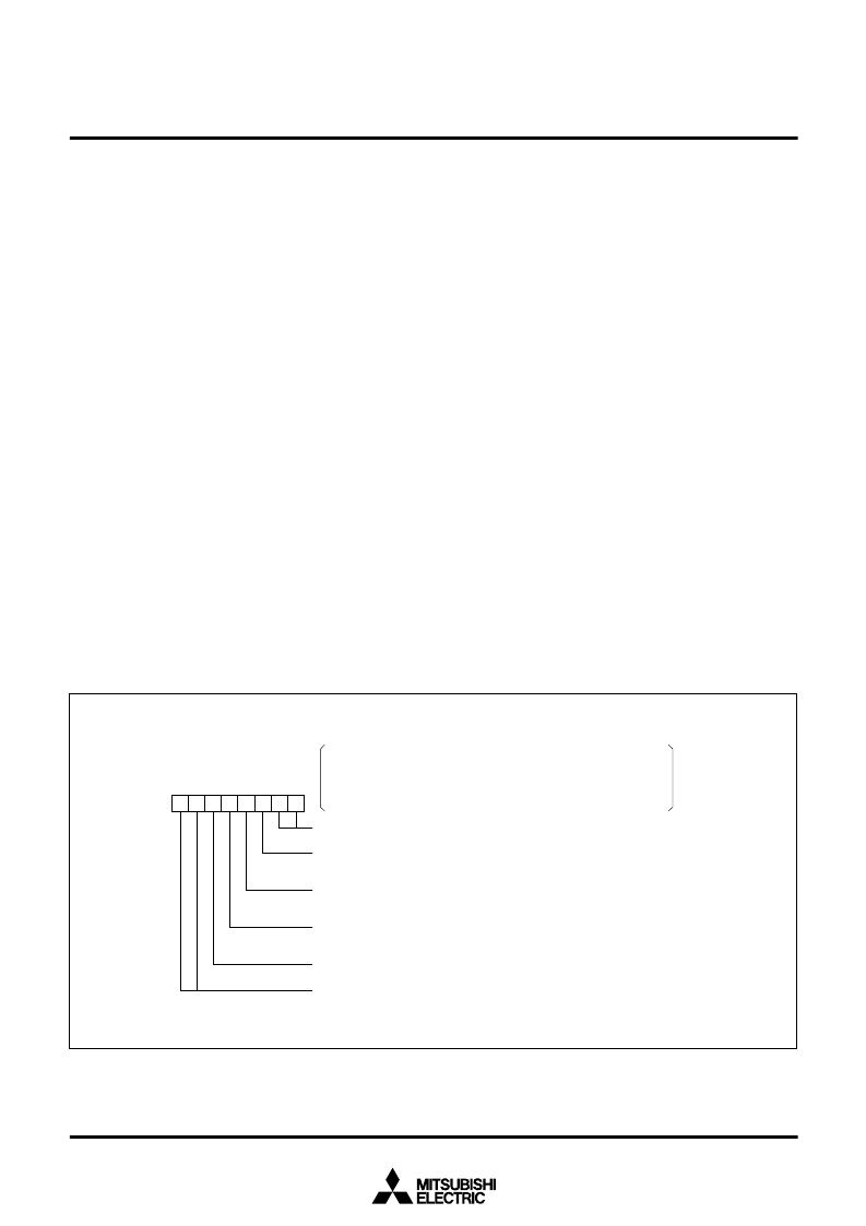
Fig. 23 Bit configuration of timer Ai mode register in event counter mode
7
×
6
×
5
0
4
3
2
1
0
0
1
0 1 : Always
“
01
”
in event counter mode
0 : No pulse output
1 : Pulse output
0 : Count at the falling edge of input signal
1 : Count at the rising edge of input signal
0 : Increment or decrement according to up/down bit
1 : Increment or decrement according to TAi
OUT
pin input signal level
0 : Always
“
0
”
in event counter mode
× ×
: Not used in event counter mode
Timer A0 mode register
Timer A1 mode register
Timer A2 mode register
Timer A3 mode register
Timer A4 mode register
Addresses
56
16
57
16
58
16
59
16
5A
16
Timer A5 mode register
Timer A6 mode register
Timer A7 mode register
Timer A8 mode register
Timer A9 mode register
Addresses
D6
16
D7
16
D8
16
D9
16
DA
16
count) or FFFF
16
(increment count), the waveform
’
s polarity is re-
versed and is output from TAi
OUT
pin.
If bit 2 is
“
0
”
, TAi
OUT
pin can be used as a normal port pin.
However, if bit 4 is
“
1
”
and the TAi
OUT
pin is used as an output pin,
the output from the pin changes the count direction. Therefore, bit 4
must be
“
0
”
unless the output from the TAi
OUT
pin is to be used to se-
lect the count direction.
Data write and data read are performed in the same way as for timer
mode. That is, when data is written to timer Ai halted, it is also writ-
ten to the reload register and the counter. When data is written to
timer Ai which is busy, the data is written to the reload register, but
not to the counter. The counter is reloaded with new data from the
reload register at the next reload time. The counter can be read at
any time.
In event counter mode, whether to increment or decrement the
counter can also be determined by supplying two kinds of pulses of
which phases differ by 90
°
to timer A2, A3, A4, A7, A8 or A9. There
are two types of two-phase pulse processing operations. One uses
timers A2, A3, A7, and A8 and the other uses timers A4 and A9. In
both processing operations, two pulses described above are input to
the TA
jOUT
(j = 2 to 4, 7 to 9) pin and TAj
IN
pin respectively.
When timers A2, A3, A7, and A8 are used, as shown in Figure 25, the
count is incremented when a rising edge is input to the TAk
IN
(k=2,
3, 7, 8) pin after the level of TAk
OUT
pin changes from
“
L
”
to
“
H
”
, and
when the falling edge is input, the count is decremented.
For timers A4 and A9, as shown in Figure 26, when a phase-related
pulse with a rising edge input to the TAl
IN
(l = 4, 9) pin is input after
the level of TAl
OUT
pin changes from
“
L
”
to
“
H
”
, the count is
incremented at the respective rising edge and falling edge of the
TAl
OUT
pin and TAl
IN
pin.
相關(guān)PDF資料 |
PDF描述 |
|---|---|
| M37905M6C-XXXFP | DIODE SCHOTTKY DUAL-DUAL SERIES 25V 200mW 0.32V-vf 200mA-IFM 1mA-IF 2uA-IR SOT-363 3K/REEL |
| M37905M6C-XXXSP | DIO, BAT54C, DUAL SHOTTKEY, COMMON CATHODE, SOT23 |
| M37905M8C-XXXFP | 16 BIT CMOS MICROCOMPUTER |
| M37905M8C-XXXSP | DIODE SCHOTTKY DUAL COMMON-CATHODE 25V 200mW 0.32V-vf 200mA-IFM 1mA-IF 2uA-IR SOT-23 3K/REEL |
| M37906F8CFP | 16-BIT CMOS MICROCOMPUTER |
相關(guān)代理商/技術(shù)參數(shù) |
參數(shù)描述 |
|---|---|
| M37905M6C-XXXFP | 制造商:MITSUBISHI 制造商全稱:Mitsubishi Electric Semiconductor 功能描述:16 BIT CMOS MICROCOMPUTER |
| M37905M6C-XXXSP | 制造商:MITSUBISHI 制造商全稱:Mitsubishi Electric Semiconductor 功能描述:16 BIT CMOS MICROCOMPUTER |
| M37905M8C-XXXFP | 制造商:MITSUBISHI 制造商全稱:Mitsubishi Electric Semiconductor 功能描述:16 BIT CMOS MICROCOMPUTER |
| M37905M8C-XXXSP | 制造商:MITSUBISHI 制造商全稱:Mitsubishi Electric Semiconductor 功能描述:16 BIT CMOS MICROCOMPUTER |
| M37905T-PRB | 功能描述:DEV POD PROBE FOR M37900T2-RPD-E RoHS:否 類別:編程器,開發(fā)系統(tǒng) >> 配件 系列:- 產(chǎn)品培訓(xùn)模塊:Lead (SnPb) Finish for COTS Obsolescence Mitigation Program RoHS指令信息:IButton RoHS Compliance Plan 標(biāo)準(zhǔn)包裝:1 系列:- 附件類型:USB 至 1-Wire? RJ11 適配器 適用于相關(guān)產(chǎn)品:1-Wire? 設(shè)備 產(chǎn)品目錄頁面:1429 (CN2011-ZH PDF) |
發(fā)布緊急采購,3分鐘左右您將得到回復(fù)。