- 您現(xiàn)在的位置:買賣IC網(wǎng) > PDF目錄370849 > M37905M4C-XXXSP (Mitsubishi Electric Corporation) 16 BIT CMOS MICROCOMPUTER PDF資料下載
參數(shù)資料
| 型號(hào): | M37905M4C-XXXSP |
| 廠商: | Mitsubishi Electric Corporation |
| 英文描述: | 16 BIT CMOS MICROCOMPUTER |
| 中文描述: | 16位CMOS微機(jī) |
| 文件頁數(shù): | 21/102頁 |
| 文件大小: | 881K |
| 代理商: | M37905M4C-XXXSP |
第1頁第2頁第3頁第4頁第5頁第6頁第7頁第8頁第9頁第10頁第11頁第12頁第13頁第14頁第15頁第16頁第17頁第18頁第19頁第20頁當(dāng)前第21頁第22頁第23頁第24頁第25頁第26頁第27頁第28頁第29頁第30頁第31頁第32頁第33頁第34頁第35頁第36頁第37頁第38頁第39頁第40頁第41頁第42頁第43頁第44頁第45頁第46頁第47頁第48頁第49頁第50頁第51頁第52頁第53頁第54頁第55頁第56頁第57頁第58頁第59頁第60頁第61頁第62頁第63頁第64頁第65頁第66頁第67頁第68頁第69頁第70頁第71頁第72頁第73頁第74頁第75頁第76頁第77頁第78頁第79頁第80頁第81頁第82頁第83頁第84頁第85頁第86頁第87頁第88頁第89頁第90頁第91頁第92頁第93頁第94頁第95頁第96頁第97頁第98頁第99頁第100頁第101頁第102頁
21
M37905M4C-XXXFP, M37905M4C-XXXSP
M37905M6C-XXXFP, M37905M6C-XXXSP
M37905M8C-XXXFP, M37905M8C-XXXSP
PRELIMINARY
Notice: This is not a final specification.
Some parametric limits are subject to change.
16-BIT CMOS MICROCOMPUTER
MITSUBISHI MICROCOMPUTERS
INTERRUPTS
Table 3 shows the interrupt sources and the corresponding interrupt
vector addresses. Reset is also handled as an interrupt source in
this section, too.
DBC and BRK instruction are interrupts used only for debugging.
Therefore, do not use these interrupts.
Interrupts other than reset, watchdog timer, zero divide, and address
matching detection all have interrupt control registers. Table 4 shows
the addresses of the interrupt control registers and Figure 13 shows
the bit configuration of the interrupt control register.
The interrupt request bit is automatically cleared by the hardware
during reset or when processing an interrupt. Also, interrupt request
bits except for that of a watchdog timer interrupt can be cleared by
software.
An INT
i
(i = 0 to 7) interrupt request is generated by an external in-
put.
INT
i
is an external interrupt; whether to cause an interrupt at the in-
put level (level sense) or at the edge (edge sense) can be selected
with the level/edge select bit. Furthermore, the polarity of the inter-
rupt input can be selected with the polarity select bit.
When using the following pins as external interrupt input pins, be
sure to clear the direction registers of the corresponding multiplexed
ports to “0”: pins P5
1
/INT
1
, P5
2
/INT
2
, P5
3
/INT
3
, P5
5
/INT
5
, P5
6
/INT
6
,
and P5
7
/INT
7
.
When the external interrupt input read register (address 95
16
), which
is shown in Figure 12, is read out, the status of pins INT
0
through
INT
7
can directly be read.
Timer and UART interrupts are described in the respective section.
The priority of interrupts when multiple interrupt requests are caused
simultaneously is partially fixed by hardware, but, it can also be ad-
justed by software as shown in Figure 14.
The hardware priority is fixed as the following:
reset > watchdog timer > other interrupts
Interrupts
UART2 transmit
UART2 receive
Timer A9
Timer A8
Timer A7
Timer A6
Timer A5
INT
7
external interrupt
INT
6
external interrupt
INT
5
external interrupt
Address matching detection interrupt
INT
4
external interrupt
INT
3
external interrupt
A-D conversion
UART1 transmit
UART1 receive
UART0 transmit
UART0 receive
Timer B2
Timer B1
Timer B0
Timer A4
Timer A3
Timer A2
Timer A1
Timer A0
INT
2
external interrupt
INT
1
external interrupt
INT
0
external interrupt
Watchdog timer
DBC (Do not select.)
Break instruction (Do not select.)
Zero divide
Reset
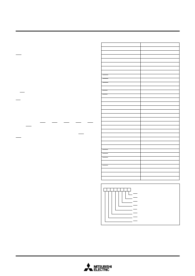
Table 3. Interrupt sources and interrupt vector addresses
Vector addresses
00FFB4
16
00FFB5
16
00FFB6
16
00FFB7
16
00FFB8
16
00FFB9
16
00FFBA
16
00FFBB
16
00FFBC
16
00FFBE
16
00FFC0
16
00FFC2
16
00FFC4
16
00FFC6
16
00FFCA
16
00FFCB
16
00FFD0
16
00FFD1
16
00FFD2
16
00FFD3
16
00FFD4
16
00FFD6
16
00FFD8
16
00FFDA
16
00FFDC
16
00FFDE
16
00FFE0
16
00FFE2
16
00FFE4
16
00FFE6
16
00FFE8
16
00FFEA
16
00FFEC
16
00FFEE
16
00FFF0
16
00FFF2
16
00FFF6
16
00FFF8
16
00FFFA
16
00FFFC
16
00FFFE
16
00FFBD
16
00FFBF
16
00FFC1
16
00FFC3
16
00FFC5
16
00FFC7
16
00FFD5
16
00FFD7
16
00FFD9
16
00FFDB
16
00FFDD
16
00FFDF
16
00FFE1
16
00FFE3
16
00FFE5
16
00FFE7
16
00FFE9
16
00FFEB
16
00FFED
16
00FFEF
16
00FFF1
16
00FFF3
16
00FFF7
16
00FFF9
16
00FFFB
16
00FFFD
16
00FFFF
16
Fig. 12 Bit configuration of external interrupt input read register
7
6
5
4
3
2
1
0
INT
0
read bit
INT
1
read bit
INT
2
read bit
INT
3
read bit
INT
4
read bit
INT
5
read bit
INT
6
read bit
INT
7
read bit
External interrupt input read register
Address
95
16
相關(guān)PDF資料 |
PDF描述 |
|---|---|
| M37905M6C-XXXFP | DIODE SCHOTTKY DUAL-DUAL SERIES 25V 200mW 0.32V-vf 200mA-IFM 1mA-IF 2uA-IR SOT-363 3K/REEL |
| M37905M6C-XXXSP | DIO, BAT54C, DUAL SHOTTKEY, COMMON CATHODE, SOT23 |
| M37905M8C-XXXFP | 16 BIT CMOS MICROCOMPUTER |
| M37905M8C-XXXSP | DIODE SCHOTTKY DUAL COMMON-CATHODE 25V 200mW 0.32V-vf 200mA-IFM 1mA-IF 2uA-IR SOT-23 3K/REEL |
| M37906F8CFP | 16-BIT CMOS MICROCOMPUTER |
相關(guān)代理商/技術(shù)參數(shù) |
參數(shù)描述 |
|---|---|
| M37905M6C-XXXFP | 制造商:MITSUBISHI 制造商全稱:Mitsubishi Electric Semiconductor 功能描述:16 BIT CMOS MICROCOMPUTER |
| M37905M6C-XXXSP | 制造商:MITSUBISHI 制造商全稱:Mitsubishi Electric Semiconductor 功能描述:16 BIT CMOS MICROCOMPUTER |
| M37905M8C-XXXFP | 制造商:MITSUBISHI 制造商全稱:Mitsubishi Electric Semiconductor 功能描述:16 BIT CMOS MICROCOMPUTER |
| M37905M8C-XXXSP | 制造商:MITSUBISHI 制造商全稱:Mitsubishi Electric Semiconductor 功能描述:16 BIT CMOS MICROCOMPUTER |
| M37905T-PRB | 功能描述:DEV POD PROBE FOR M37900T2-RPD-E RoHS:否 類別:編程器,開發(fā)系統(tǒng) >> 配件 系列:- 產(chǎn)品培訓(xùn)模塊:Lead (SnPb) Finish for COTS Obsolescence Mitigation Program RoHS指令信息:IButton RoHS Compliance Plan 標(biāo)準(zhǔn)包裝:1 系列:- 附件類型:USB 至 1-Wire? RJ11 適配器 適用于相關(guān)產(chǎn)品:1-Wire? 設(shè)備 產(chǎn)品目錄頁面:1429 (CN2011-ZH PDF) |
發(fā)布緊急采購,3分鐘左右您將得到回復(fù)。