- 您現(xiàn)在的位置:買賣IC網(wǎng) > PDF目錄98005 > M34524MC-XXXFP 4-BIT, MROM, 6 MHz, MICROCONTROLLER, PQFP64 PDF資料下載
參數(shù)資料
| 型號: | M34524MC-XXXFP |
| 元件分類: | 微控制器/微處理器 |
| 英文描述: | 4-BIT, MROM, 6 MHz, MICROCONTROLLER, PQFP64 |
| 封裝: | 14 X 14 MM, 0.80 MM PITCH, PLASTIC, QFP-64 |
| 文件頁數(shù): | 138/163頁 |
| 文件大小: | 1235K |
| 代理商: | M34524MC-XXXFP |
第1頁第2頁第3頁第4頁第5頁第6頁第7頁第8頁第9頁第10頁第11頁第12頁第13頁第14頁第15頁第16頁第17頁第18頁第19頁第20頁第21頁第22頁第23頁第24頁第25頁第26頁第27頁第28頁第29頁第30頁第31頁第32頁第33頁第34頁第35頁第36頁第37頁第38頁第39頁第40頁第41頁第42頁第43頁第44頁第45頁第46頁第47頁第48頁第49頁第50頁第51頁第52頁第53頁第54頁第55頁第56頁第57頁第58頁第59頁第60頁第61頁第62頁第63頁第64頁第65頁第66頁第67頁第68頁第69頁第70頁第71頁第72頁第73頁第74頁第75頁第76頁第77頁第78頁第79頁第80頁第81頁第82頁第83頁第84頁第85頁第86頁第87頁第88頁第89頁第90頁第91頁第92頁第93頁第94頁第95頁第96頁第97頁第98頁第99頁第100頁第101頁第102頁第103頁第104頁第105頁第106頁第107頁第108頁第109頁第110頁第111頁第112頁第113頁第114頁第115頁第116頁第117頁第118頁第119頁第120頁第121頁第122頁第123頁第124頁第125頁第126頁第127頁第128頁第129頁第130頁第131頁第132頁第133頁第134頁第135頁第136頁第137頁當(dāng)前第138頁第139頁第140頁第141頁第142頁第143頁第144頁第145頁第146頁第147頁第148頁第149頁第150頁第151頁第152頁第153頁第154頁第155頁第156頁第157頁第158頁第159頁第160頁第161頁第162頁第163頁
Rev.2.00
Jul 27, 2004
page 74 of 159
REJ03B0091-0200Z
4524 Group
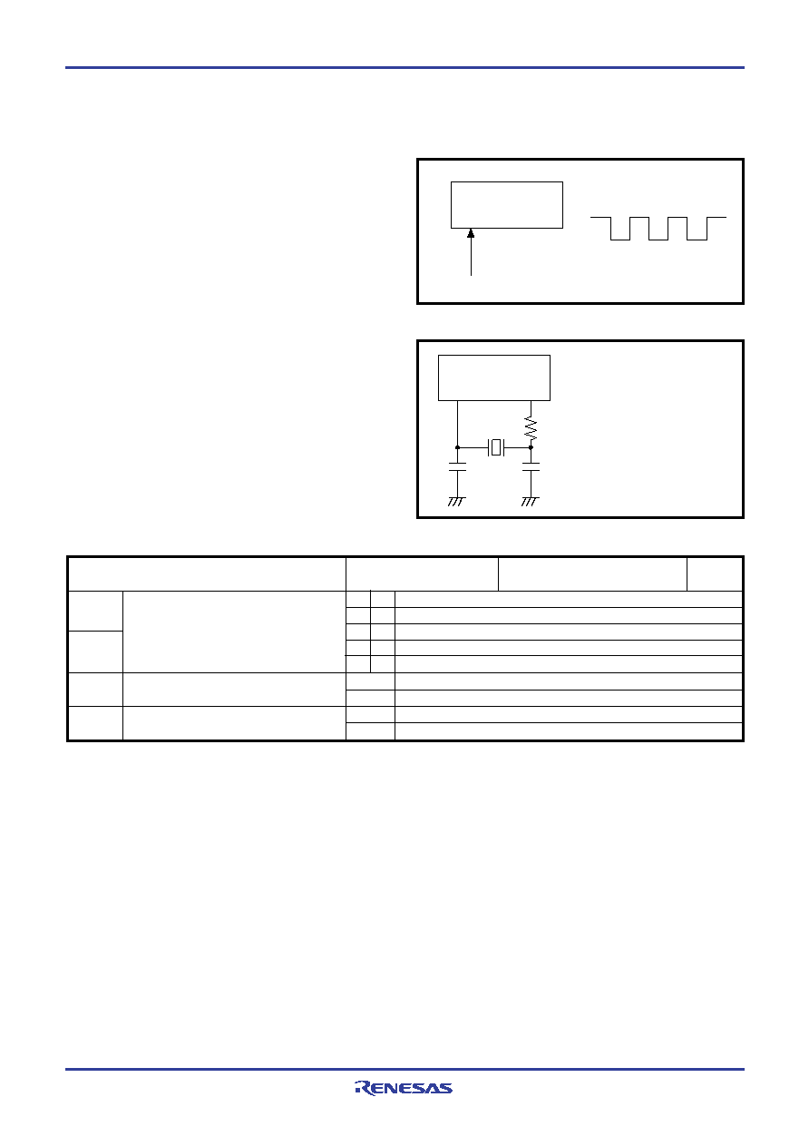
(5) External clock
When the external clock signal is used as the main clock (f(XIN)),
connect the XIN pin to the clock source and leave XOUT pin open.
Then, execute the CMCK instruction (Figure 63).
Be careful that the maximum value of the oscillation frequency
when using the external clock differs from the value when using the
ceramic resonator (refer to the recommended operating condition).
Also, note that the power down function (POF or POF2 instruction)
cannot be used when using the external clock.
(6) Sub-clock generating circuit f(XCIN)
The quartz-crystal oscillator can be used for the sub-clock signal
f(XCIN). Connect a quartz-crystal oscillator and this external circuit
to pins XCIN and XCOUT at the shortest distance. A feedback resis-
tor is built in between pins XCIN and XCOUT (Figure 64).
(7) Clock control register MR
Register MR controls system clock. Set the contents of this register
through register A with the TMRA instruction. In addition, the TAMR
instruction can be used to transfer the contents of register MR to
register A.
Table 24 Clock control register MR
Fig. 63 External clock input circuit
Note : “R” represents read enabled, and “W” represents write enabled.
M34524
XIN
XOUT
External oscillation circuit
VDD
VSS
Execute the CMCK
instruction in program.
*
Fig. 64 External quartz-crystal circuit
M34524
XCIN
XCOUT
Rd
CIN
COUT
MR3
Clock control register MR
Operation mode
Through mode (frequency not divided)
Frequency divided by 2 mode
Frequency divided by 4 mode
Frequency divided by 8 mode
Main clock oscillation enabled
Main clock oscillation stop
Main clock (f(XIN) or f(RING))
Sub-clock (f(XCIN))
at reset : 11002
at power down : state retained
MR3
0
1
R/W
TAMR/
TMRA
Main clock oscillation circuit control bit
System clock selection bit
Operation mode selection bits
0
1
0
1
MR2
0
1
0
1
MR1
MR0
MR2
ROM ORDERING METHOD
1.Mask ROM Order Confirmation Form
2.Mark Specification Form
3.Data to be written to ROM, in EPROM form (three identical cop-
ies) or one floppy disk.
For the mask ROM confirmation and the mark specifications, re-
fer to the “Renesas Technology Corp.” Homepage
(http://www.renesas.com/en/rom).
Note: Externally connect a damping
resistor Rd depending on the
oscillation frequency.
(A feedback resistor is built-in.)
Use the quartz-crystal manu-
facturer’s recommended value
because constants such as ca-
pacitance depend on the
resonator.
相關(guān)PDF資料 |
PDF描述 |
|---|---|
| M34524MC-XXXFP | 4-BIT, MROM, 6 MHz, MICROCONTROLLER, PQFP64 |
| M34550E8FS | 4-BIT, UVPROM, 1.6 MHz, MICROCONTROLLER, CQCC80 |
| M34551E8-XXXFP | 4-BIT, OTPROM, MICROCONTROLLER, PQFP48 |
| M34554M8-XXXFP | 4-BIT, MROM, 6 MHz, MICROCONTROLLER, PQFP64 |
| M34554MC-XXXFP | 4-BIT, MROM, 6 MHz, MICROCONTROLLER, PQFP64 |
相關(guān)代理商/技術(shù)參數(shù) |
參數(shù)描述 |
|---|---|
| M3452-C09K1 | 制造商:Bonitron 功能描述:OVERVOLTAGE BRAKING TRANSISTOR |
| M3452-C125K2 | 制造商:Bonitron 功能描述:OVERVOLTAGE BRAKING TRANSISTOR |
| M3452-C125K2,A | 制造商:Bonitron 功能描述:OVERVOLTAGE BRAKING TRANSISTOR |
| M3452-C150B7 | 制造商:Bonitron 功能描述:OVERVOLTAGE BRAKING TRANSISTOR |
| M3452-C150B7-A | 制造商:Bonitron 功能描述:OVERVOLTAGE BRAKING TRANSISTOR |
發(fā)布緊急采購,3分鐘左右您將得到回復(fù)。