- 您現(xiàn)在的位置:買(mǎi)賣(mài)IC網(wǎng) > PDF目錄299403 > LFXP2-17E-7F484C (LATTICE SEMICONDUCTOR CORP) PDF資料下載
參數(shù)資料
| 型號(hào): | LFXP2-17E-7F484C |
| 廠(chǎng)商: | LATTICE SEMICONDUCTOR CORP |
| 元件分類(lèi): | FPGA |
| 中文描述: | FPGA, 420 MHz, PBGA484 |
| 封裝: | 23 X 23 MM, FPBGA-484 |
| 文件頁(yè)數(shù): | 30/92頁(yè) |
| 文件大小: | 1701K |
| 代理商: | LFXP2-17E-7F484C |
第1頁(yè)第2頁(yè)第3頁(yè)第4頁(yè)第5頁(yè)第6頁(yè)第7頁(yè)第8頁(yè)第9頁(yè)第10頁(yè)第11頁(yè)第12頁(yè)第13頁(yè)第14頁(yè)第15頁(yè)第16頁(yè)第17頁(yè)第18頁(yè)第19頁(yè)第20頁(yè)第21頁(yè)第22頁(yè)第23頁(yè)第24頁(yè)第25頁(yè)第26頁(yè)第27頁(yè)第28頁(yè)第29頁(yè)當(dāng)前第30頁(yè)第31頁(yè)第32頁(yè)第33頁(yè)第34頁(yè)第35頁(yè)第36頁(yè)第37頁(yè)第38頁(yè)第39頁(yè)第40頁(yè)第41頁(yè)第42頁(yè)第43頁(yè)第44頁(yè)第45頁(yè)第46頁(yè)第47頁(yè)第48頁(yè)第49頁(yè)第50頁(yè)第51頁(yè)第52頁(yè)第53頁(yè)第54頁(yè)第55頁(yè)第56頁(yè)第57頁(yè)第58頁(yè)第59頁(yè)第60頁(yè)第61頁(yè)第62頁(yè)第63頁(yè)第64頁(yè)第65頁(yè)第66頁(yè)第67頁(yè)第68頁(yè)第69頁(yè)第70頁(yè)第71頁(yè)第72頁(yè)第73頁(yè)第74頁(yè)第75頁(yè)第76頁(yè)第77頁(yè)第78頁(yè)第79頁(yè)第80頁(yè)第81頁(yè)第82頁(yè)第83頁(yè)第84頁(yè)第85頁(yè)第86頁(yè)第87頁(yè)第88頁(yè)第89頁(yè)第90頁(yè)第91頁(yè)第92頁(yè)
2-33
Architecture
Lattice Semiconductor
LatticeXP2 Family Data Sheet
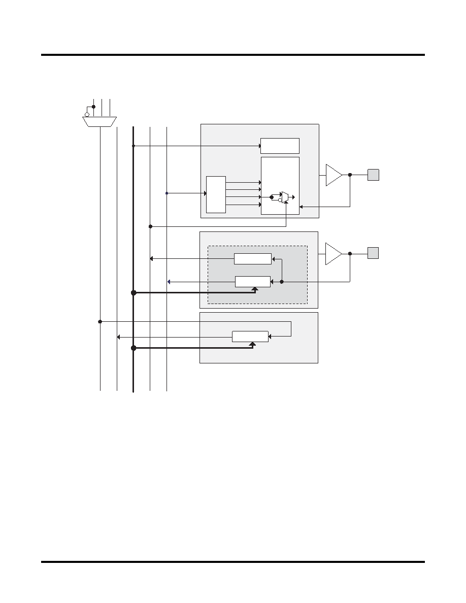
Figure 2-31. DQS Local Bus
Polarity Control Logic
In a typical DDR memory interface design, the phase relationship between the incoming delayed DQS strobe and
the internal system clock (during the READ cycle) is unknown. The LatticeXP2 family contains dedicated circuits to
transfer data between these domains. To prevent set-up and hold violations, at the domain transfer between DQS
(delayed) and the system clock, a clock polarity selector is used. This changes the edge on which the data is regis-
tered in the synchronizing registers in the input register block and requires evaluation at the start of each READ
cycle for the correct clock polarity.
Prior to the READ operation in DDR memories, DQS is in tristate (pulled by termination). The DDR memory device
drives DQS low at the start of the preamble state. A dedicated circuit detects this transition. This signal is used to
control the polarity of the clock to the synchronizing registers.
sysIO
Buffer
DDR
Datain
PAD
DI
CLK1
CEI
PIO
sysIO
Buffer
GSR
DQS
To Sync
Reg.
DQS
To DDR
Reg.
DQS
Strobe
PAD
PIO
DQSDEL
Polarity Control
Logic
DQS
Calibration bus
from DLL
DQSXFER
Output
Register Block
Input
Register Block
DQSXFER
DCNTL[6:0]
Polarit
y
control
DQS
DI
DQSXFERDEL*
DQSXFER
DCNTL[6:0]
*DQSXFERDEL shifts ECLK1 by 90% and is not associated with a particular PIO.
DCNTL[6:0]
ECLK1
CLK1
ECLK2
ECLK1
相關(guān)PDF資料 |
PDF描述 |
|---|---|
| LFXP20E-3FN484C | |
| LFXP20E-5FN484C | |
| LFXP15C-4FN256C | |
| LFZ3508VXX | GENERAL PURPOSE INDUCTOR |
| LFZ2805HXX | GENERAL PURPOSE INDUCTOR |
相關(guān)代理商/技術(shù)參數(shù) |
參數(shù)描述 |
|---|---|
| LFXP2-17E-7F484C8W | 功能描述:FPGA - 現(xiàn)場(chǎng)可編程門(mén)陣列 17KLUTs 358I/O Inst- on DSP 1.2V -7Spd RoHS:否 制造商:Altera Corporation 系列:Cyclone V E 柵極數(shù)量: 邏輯塊數(shù)量:943 內(nèi)嵌式塊RAM - EBR:1956 kbit 輸入/輸出端數(shù)量:128 最大工作頻率:800 MHz 工作電源電壓:1.1 V 最大工作溫度:+ 70 C 安裝風(fēng)格:SMD/SMT 封裝 / 箱體:FBGA-256 |
| LFXP2-17E-7FN484C | 功能描述:FPGA - 現(xiàn)場(chǎng)可編程門(mén)陣列 17KLUTs 358 I/O Inst -on DSP 1.2V -6 Spd RoHS:否 制造商:Altera Corporation 系列:Cyclone V E 柵極數(shù)量: 邏輯塊數(shù)量:943 內(nèi)嵌式塊RAM - EBR:1956 kbit 輸入/輸出端數(shù)量:128 最大工作頻率:800 MHz 工作電源電壓:1.1 V 最大工作溫度:+ 70 C 安裝風(fēng)格:SMD/SMT 封裝 / 箱體:FBGA-256 |
| LFXP2-17E-7FN484C8W | 功能描述:FPGA - 現(xiàn)場(chǎng)可編程門(mén)陣列 17KLUTs 358I/O Inst -on DSP 1.2V -7 Spd RoHS:否 制造商:Altera Corporation 系列:Cyclone V E 柵極數(shù)量: 邏輯塊數(shù)量:943 內(nèi)嵌式塊RAM - EBR:1956 kbit 輸入/輸出端數(shù)量:128 最大工作頻率:800 MHz 工作電源電壓:1.1 V 最大工作溫度:+ 70 C 安裝風(fēng)格:SMD/SMT 封裝 / 箱體:FBGA-256 |
| LFXP2-17E-7FT256C | 功能描述:FPGA - 現(xiàn)場(chǎng)可編程門(mén)陣列 17KLUTs 201 I/O Inst -on DSP 1.2V -7 Spd RoHS:否 制造商:Altera Corporation 系列:Cyclone V E 柵極數(shù)量: 邏輯塊數(shù)量:943 內(nèi)嵌式塊RAM - EBR:1956 kbit 輸入/輸出端數(shù)量:128 最大工作頻率:800 MHz 工作電源電壓:1.1 V 最大工作溫度:+ 70 C 安裝風(fēng)格:SMD/SMT 封裝 / 箱體:FBGA-256 |
| LFXP2-17E-7FT256C8W | 功能描述:FPGA - 現(xiàn)場(chǎng)可編程門(mén)陣列 17KLUTs 201 I/O Inst -on DSP 1.2V -7 Spd RoHS:否 制造商:Altera Corporation 系列:Cyclone V E 柵極數(shù)量: 邏輯塊數(shù)量:943 內(nèi)嵌式塊RAM - EBR:1956 kbit 輸入/輸出端數(shù)量:128 最大工作頻率:800 MHz 工作電源電壓:1.1 V 最大工作溫度:+ 70 C 安裝風(fēng)格:SMD/SMT 封裝 / 箱體:FBGA-256 |
發(fā)布緊急采購(gòu),3分鐘左右您將得到回復(fù)。