- 您現(xiàn)在的位置:買賣IC網(wǎng) > PDF目錄299403 > LFXP2-17E-7F484C (LATTICE SEMICONDUCTOR CORP) PDF資料下載
參數(shù)資料
| 型號(hào): | LFXP2-17E-7F484C |
| 廠商: | LATTICE SEMICONDUCTOR CORP |
| 元件分類: | FPGA |
| 中文描述: | FPGA, 420 MHz, PBGA484 |
| 封裝: | 23 X 23 MM, FPBGA-484 |
| 文件頁(yè)數(shù): | 21/92頁(yè) |
| 文件大?。?/td> | 1701K |
| 代理商: | LFXP2-17E-7F484C |
第1頁(yè)第2頁(yè)第3頁(yè)第4頁(yè)第5頁(yè)第6頁(yè)第7頁(yè)第8頁(yè)第9頁(yè)第10頁(yè)第11頁(yè)第12頁(yè)第13頁(yè)第14頁(yè)第15頁(yè)第16頁(yè)第17頁(yè)第18頁(yè)第19頁(yè)第20頁(yè)當(dāng)前第21頁(yè)第22頁(yè)第23頁(yè)第24頁(yè)第25頁(yè)第26頁(yè)第27頁(yè)第28頁(yè)第29頁(yè)第30頁(yè)第31頁(yè)第32頁(yè)第33頁(yè)第34頁(yè)第35頁(yè)第36頁(yè)第37頁(yè)第38頁(yè)第39頁(yè)第40頁(yè)第41頁(yè)第42頁(yè)第43頁(yè)第44頁(yè)第45頁(yè)第46頁(yè)第47頁(yè)第48頁(yè)第49頁(yè)第50頁(yè)第51頁(yè)第52頁(yè)第53頁(yè)第54頁(yè)第55頁(yè)第56頁(yè)第57頁(yè)第58頁(yè)第59頁(yè)第60頁(yè)第61頁(yè)第62頁(yè)第63頁(yè)第64頁(yè)第65頁(yè)第66頁(yè)第67頁(yè)第68頁(yè)第69頁(yè)第70頁(yè)第71頁(yè)第72頁(yè)第73頁(yè)第74頁(yè)第75頁(yè)第76頁(yè)第77頁(yè)第78頁(yè)第79頁(yè)第80頁(yè)第81頁(yè)第82頁(yè)第83頁(yè)第84頁(yè)第85頁(yè)第86頁(yè)第87頁(yè)第88頁(yè)第89頁(yè)第90頁(yè)第91頁(yè)第92頁(yè)
2-25
Architecture
Lattice Semiconductor
LatticeXP2 Family Data Sheet
IPexpress
The user can access the sysDSP block via the ispLEVER IPexpress tool, which provides the option to configure
each DSP module (or group of modules), or by direct HDL instantiation. In addition, Lattice has partnered with The
MathWorks
to support instantiation in the Simulink tool, a graphical simulation environment. Simulink works with
ispLEVER to dramatically shorten the DSP design cycle in Lattice FPGAs.
Optimized DSP Functions
Lattice provides a library of optimized DSP IP functions. Some of the IP cores planned for the LatticeXP2 DSP
include the Bit Correlator, FFT functions, FIR Filter, Reed-Solomon Encoder/Decoder, Turbo Encoder/Decoder and
Convolutional Encoder/Decoder. Please contact Lattice to obtain the latest list of available DSP IP cores.
Resources Available in the LatticeXP2 Family
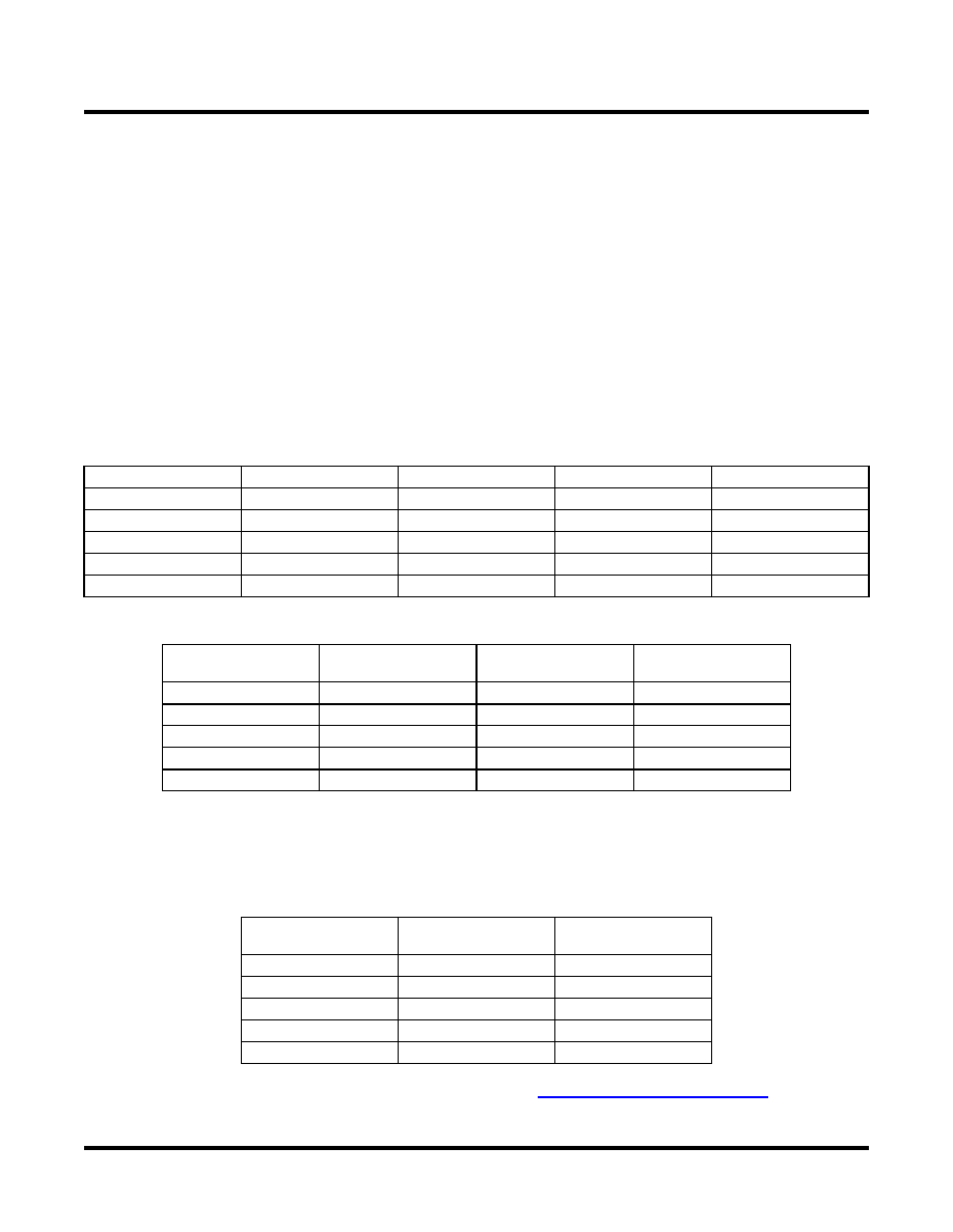
Table 2-8 shows the maximum number of multipliers for each member of the LatticeXP2 family. Table 2-9 shows the
maximum available EBR RAM Blocks and Serial TAG Memory bits in each LatticeXP2 device. EBR blocks,
together with Distributed RAM can be used to store variables locally for fast DSP operations.
Table 2-8. Maximum Number of DSP Blocks in the LatticeXP2 Family
Table 2-9. Embedded SRAM/TAG Memory in the LatticeXP2 Family
LatticeXP2 DSP Performance
Table 2-10 lists the maximum performance in Millions of MAC (MMAC) operations per second for each member of
the LatticeXP2 family.
Table 2-10. DSP Performance
For further information on the sysDSP block, please see TN1140, LatticeXP2 sysDSP Usage Guide.
Device
DSP Block
9x9 Multiplier
18x18 Multiplier
36x36 Multiplier
XP2-5
3
24
12
3
XP2-8
4
32
16
4
XP2-17
5
40
20
5
XP2-30
7
56
28
7
XP2-40
8
64
32
8
Device
EBR SRAM Block
Total EBR SRAM
(Kbits)
TAG Memory
(Bits)
XP2-5
9
166
632
XP2-8
12
221
768
XP2-17
15
276
2184
XP2-30
21
387
2640
XP2-40
48
885
3384
Device
DSP Block
DSP Performance
MMAC
XP2-5
3
3,900
XP2-8
4
5,200
XP2-17
5
6,500
XP2-30
7
9,100
XP2-40
8
10,400
相關(guān)PDF資料 |
PDF描述 |
|---|---|
| LFXP20E-3FN484C | |
| LFXP20E-5FN484C | |
| LFXP15C-4FN256C | |
| LFZ3508VXX | GENERAL PURPOSE INDUCTOR |
| LFZ2805HXX | GENERAL PURPOSE INDUCTOR |
相關(guān)代理商/技術(shù)參數(shù) |
參數(shù)描述 |
|---|---|
| LFXP2-17E-7F484C8W | 功能描述:FPGA - 現(xiàn)場(chǎng)可編程門陣列 17KLUTs 358I/O Inst- on DSP 1.2V -7Spd RoHS:否 制造商:Altera Corporation 系列:Cyclone V E 柵極數(shù)量: 邏輯塊數(shù)量:943 內(nèi)嵌式塊RAM - EBR:1956 kbit 輸入/輸出端數(shù)量:128 最大工作頻率:800 MHz 工作電源電壓:1.1 V 最大工作溫度:+ 70 C 安裝風(fēng)格:SMD/SMT 封裝 / 箱體:FBGA-256 |
| LFXP2-17E-7FN484C | 功能描述:FPGA - 現(xiàn)場(chǎng)可編程門陣列 17KLUTs 358 I/O Inst -on DSP 1.2V -6 Spd RoHS:否 制造商:Altera Corporation 系列:Cyclone V E 柵極數(shù)量: 邏輯塊數(shù)量:943 內(nèi)嵌式塊RAM - EBR:1956 kbit 輸入/輸出端數(shù)量:128 最大工作頻率:800 MHz 工作電源電壓:1.1 V 最大工作溫度:+ 70 C 安裝風(fēng)格:SMD/SMT 封裝 / 箱體:FBGA-256 |
| LFXP2-17E-7FN484C8W | 功能描述:FPGA - 現(xiàn)場(chǎng)可編程門陣列 17KLUTs 358I/O Inst -on DSP 1.2V -7 Spd RoHS:否 制造商:Altera Corporation 系列:Cyclone V E 柵極數(shù)量: 邏輯塊數(shù)量:943 內(nèi)嵌式塊RAM - EBR:1956 kbit 輸入/輸出端數(shù)量:128 最大工作頻率:800 MHz 工作電源電壓:1.1 V 最大工作溫度:+ 70 C 安裝風(fēng)格:SMD/SMT 封裝 / 箱體:FBGA-256 |
| LFXP2-17E-7FT256C | 功能描述:FPGA - 現(xiàn)場(chǎng)可編程門陣列 17KLUTs 201 I/O Inst -on DSP 1.2V -7 Spd RoHS:否 制造商:Altera Corporation 系列:Cyclone V E 柵極數(shù)量: 邏輯塊數(shù)量:943 內(nèi)嵌式塊RAM - EBR:1956 kbit 輸入/輸出端數(shù)量:128 最大工作頻率:800 MHz 工作電源電壓:1.1 V 最大工作溫度:+ 70 C 安裝風(fēng)格:SMD/SMT 封裝 / 箱體:FBGA-256 |
| LFXP2-17E-7FT256C8W | 功能描述:FPGA - 現(xiàn)場(chǎng)可編程門陣列 17KLUTs 201 I/O Inst -on DSP 1.2V -7 Spd RoHS:否 制造商:Altera Corporation 系列:Cyclone V E 柵極數(shù)量: 邏輯塊數(shù)量:943 內(nèi)嵌式塊RAM - EBR:1956 kbit 輸入/輸出端數(shù)量:128 最大工作頻率:800 MHz 工作電源電壓:1.1 V 最大工作溫度:+ 70 C 安裝風(fēng)格:SMD/SMT 封裝 / 箱體:FBGA-256 |
發(fā)布緊急采購(gòu),3分鐘左右您將得到回復(fù)。